Intel
®
EP80579 Integrated Processor Product Line May 2010
Order Number: 320068-005US 338
System Memory Interface (Memory Down)—Intel
®
EP80579 Integrated Processor Product Line
B.6 Overview and Design Considerations
There are two length constraints placed on each signal group within the DDR2
interface:
• Absolute length: These constraints define the length range over which the signals
will meet signal integrity rules.
• Clock and strobe length matching: These constraints ensure that clock-relative AC
timing margins are met.
Intel recommends following a preliminary test route to establish the natural bounds on
all signal groups. This route defines the target lengths for each signal group, and
provides an acceptable solution space when the length matching formulas are applied.
Use the EP80579 Memory Down Trace Length Calculator (TLC) to ensure that the
length and matching requirements are properly met.
B.6.1 Length Matching and Length Formulas
The routing guidelines provided in the following subsections define the recommended
routing topologies, trace width and spacing geometries, and absolute minimum and
maximum routed lengths for each signal group, which are recommended to achieve
optimal signal integrity and timing. In addition to the absolute length limits provided in
the individual guideline tables, more restrictive length matching formulas are also
provided that further restrict the minimum and maximum length range of each signal
group with respect to clock, within the overall boundaries defined in the guidelines
tables, as required to guarantee timing margins. These secondary constraints are
referred to as length matching constraints and the formulas used are referred to as
length matching formulas.
All signal groups are length matched to the DDR2 clocks, with the clocks themselves
length tuned to a fixed length across the Memory Down devices. The amount of
minimum to maximum length variance allowed for each signal group around the clock
reference length varies from signal group to signal group depending on the amount of
timing variance that can be tolerated. A simplified summary of the length matching
formulas from the EP80579 to the Memory Down devices for each signal group is
provided in Table B-26.
Note: All length matching formulas are based on the EP80579 die-pad to Memory Down pin
total length.
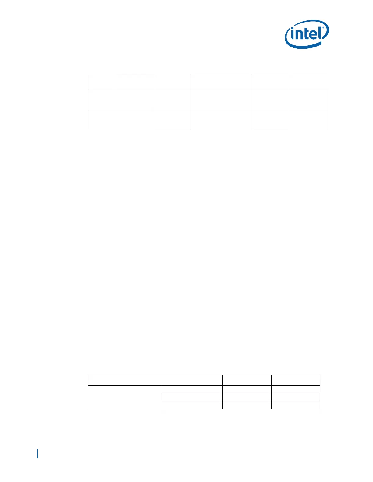
Table B-25. Memory Configurations Supported by the EP80579
Config
No.
Topology Ranks
Memory Down (x8)
Device Placement
Memory
Device Width
Figures
1
Memory Down
on PCB
(1 chip select)
One
8 on Top
or
8 on Bottom
8
2
Memory Down
on PCB
(1 chip select)
One
4 on Top
and
4 on Bottom
8
Table B-26. Length Matching Formulas for Memory Down Configuration
Source to Destination Signal Group Minimum Length Maximum Length
EP80579 to Memory Down Pin
ADDR/CMD/CTRL to Clock Clock - 0 mils Clock + 30 mils
Strobe to Clock Clock - 500 mils Clock + 500 mils
Data to Strobe Strobe - 20 mils Strobe + 20 mils