Intel
®
EP80579 Integrated Processor Product Line May 2010
Order Number: 320068-005US 312
Schematics Checklist—Intel
®
EP80579 Integrated Processor Product Line
28.4 CK410 Schematic Checklist
For additional information, see the CK410 Clock Synthesizer/Driver Specification and
the component’s datasheet.
Bandgap Power Pins with Filter
Note: See Section 6.6.5 and Table 13 for Bandgap Filter guidelines
VCCASATABG3P3 PWR
3.3V SATA Bandgap power
supply
• connect to 3.3V
(VCC33) with
bandgap filter
VCCABG3P3_USB PWR
3.3V USB Bandgap power
supply
• connect to 3.3V
(VCC33) with
bandgap filter
VCCABGP033 PWR
3.3V PCI Express
Bandgap power supply
• connect to 3.3V
(VCC33) with
bandgap filter
Ground Pins
VSSA GND Analog Ground • The Analog Ground
(VSSA) should be
isolated from the normal
Ground (VSS) on the
Platform
• The Analog Ground
(VSSA) should be
referenced to CRU PLL
Power supply
(VCCAHPLL).
• VSSA and VSS are
connected together
internally in the device
VSS GND Ground
Table 101. Decoupling Recommendations (Sheet 3 of 3)
Power/Ground
Pin Name
Type Configuration Decap Qty Component Layout Notes
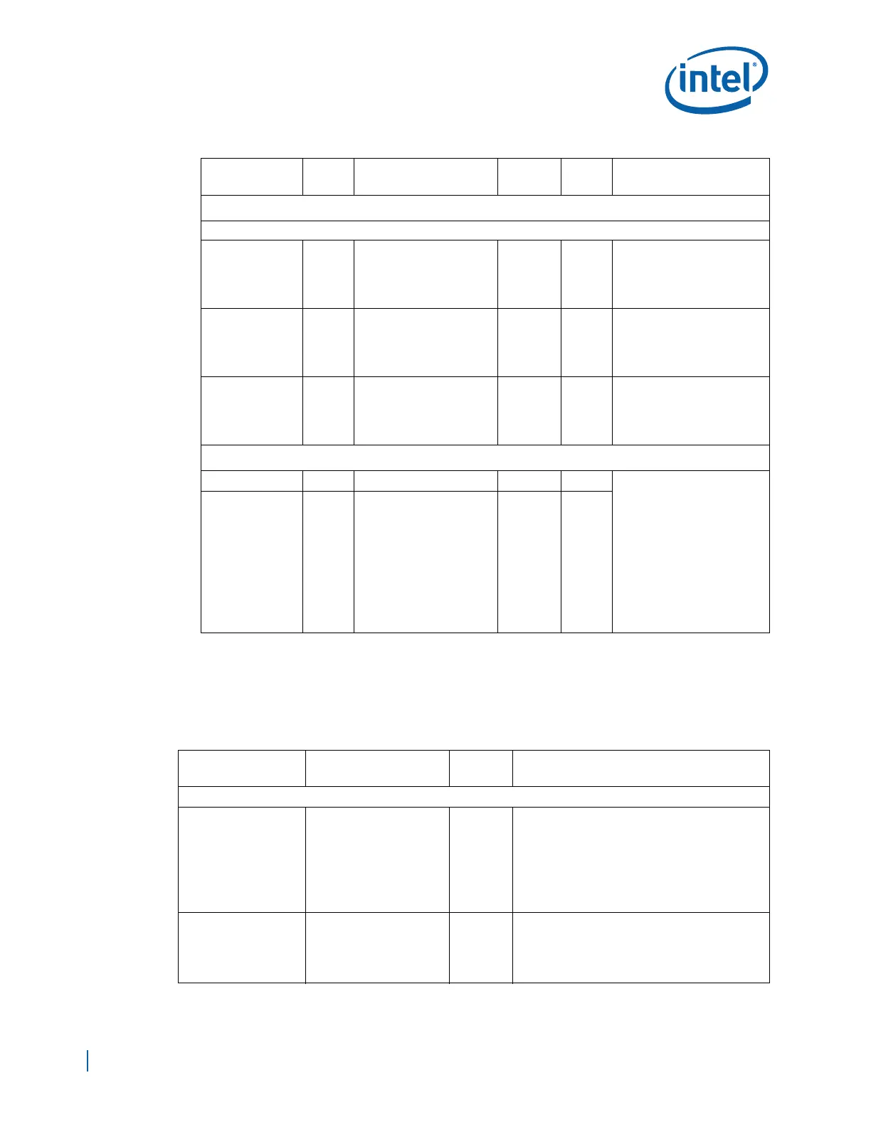
Table 102. CK410 Schematic Checklist (Sheet 1 of 3)
Pin Name
System
Pull-up/Pull-down
Series
Resistor
Recommendations
Note: See the CK410 Clock Synthesizer/Driver Specification for more details
PCIF_0/ITP_EN
•4.7 KΩ pull-up to
Platform 3.3V (VCC3)
for ITPCLK
•4.7 KΩ pull-down to
GND for SRC_7
33 Ω±1%
• On the Development Board, this pin is pulled
high using a 4.7 KΩ resistor to VCC3 to
select pins 35 and 36 as ITPCLK.
• Customer can use this pin as a PCIF as well.
• If used as a PCIF clock as well use multiple
33 Ω±1% series resistors for isolation if the
clock signal is shared between multiple
devices.
PCIF_1,
PCIF_2
33 Ω±1%
Free running PCI Clock Outputs
• If not used, can be left as NC.
• If used as a PCIF clock use multiple 33
Ω±1% series resistor if the clock signal is
shared between multiple devices.

 Loading...


