Intel
®
EP80579 Integrated Processor Product Line—Schematics Checklist
Intel
®
EP80579 Integrated Processor Product Line
Platform Design Guide May 2010
313 Order Number: 320068-005US
SRC[6:1]/SRC[6:1]#
49.9 Ω±1% pull-down to
GND
33 Ω±5%
100 MHz Differential Clocks Outputs
• Connect to various differential serial
reference clocks (PCI-E, SATA, etc.)
• If not used, can be left as NC.
DOT96/DOT96#
49.9 Ω±1% pull-down to
GND
33 Ω±5%
96 MHz Differential Clock Output
• If not used, can be left as NC
PCI[5:0] 33 Ω±1%
33 MHz single-ended PCI Clock Outputs
• If not used, can be left as NC.
• Use multiple 33 Ω±1% series resistor if the
clock signal is shared between multiple
devices.
CPU[1:0]/CPU[1:0]#
49.9 Ω±1% pull-down to
GND
33 Ω±5%
100/133 MHz EP80579 Core Differential Clock
• Connect CPU_0 to EP80579 CLKP100
• Connect CPU_0# to EP80579 CLKN100
• Leave unused clocks as NC
CPU_2/SRC_7,
CPU_2#/SRC_7#
49.9 Ω±1% pull-down to
GND
33 Ω±5%
Selectable Differential CPU or SRC output
• If on-board XDP/ITP is implemented, this
pair of clock signals is used for the XDP/ITP
connector. Otherwise, it can be routed to the
dedicated XDP/ITP clock pins on the
processor socket. If no on-board ITP, then
this can be used for SRC7.
• If not used, can be left as NC
FS_A 1KΩ ±1% pull-up to VCC3
• This pin works in conjunction with FS_B and
FS_C to select the CPU clock frequency
Note: See the CK410 Clock Synthesizer/Driver
Specification for more details
FS_B/TEST_MODE
1KΩ ±1% pull-down to
GND
• This pin works in conjunction with FS_A and
FS_C to select the CPU clock frequency
Note: See the CK410 Clock Synthesizer/Driver
Specification for more details
FS_C/TEST_SEL
Clk Frequency Strapping
Options:
• If BSEL = 0 (FSB =
400MTS), connect to
VCC3 through 1KΩ
±1% resistor
• If BSEL = 1 (FSB =
533MTS), connect to
GND through 1KΩ
±1% resistor
• This pin works in conjunction with FS_A and
FS_B to select the CPU clock frequency.
• Connect using EP80579 BSEL signal to select
EP80579 FSB frequency
Note: See the CK410 Clock Synthesizer/Driver
Specification for more details
REF 33 Ω±5%
14.318 MHz reference clock output
• Can connect to various reference clock
devices (ICH, SIO, LPC, etc.)
• The REF signal can support 1-3 devices,
• Use multiple 33 Ω±1% series resistors to
isolate clocks if the clock signal is shared
between multiple devices.
• Use a clock buffer if the clock signal
connects to four or more devices.
IREF
475 Ω ±1% pull-down to
GND
• A precision resistor (internal) is attached to
this pin, which is connected to the internal
current reference.
• Connect a 475 Ω ±1% pull-down resistor to
this pin
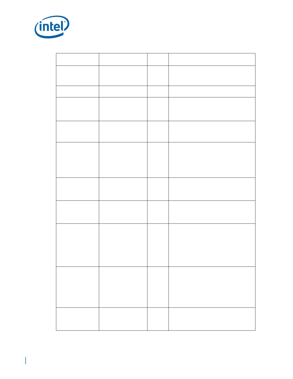
Table 102. CK410 Schematic Checklist (Sheet 2 of 3)
Pin Name
System
Pull-up/Pull-down
Series
Resistor
Recommendations

 Loading...


