Intel
®
EP80579 Integrated Processor Product Line May 2010
Order Number: 320068-005US 35
Baseboard Requirements—Intel
®
EP80579 Integrated Processor Product Line
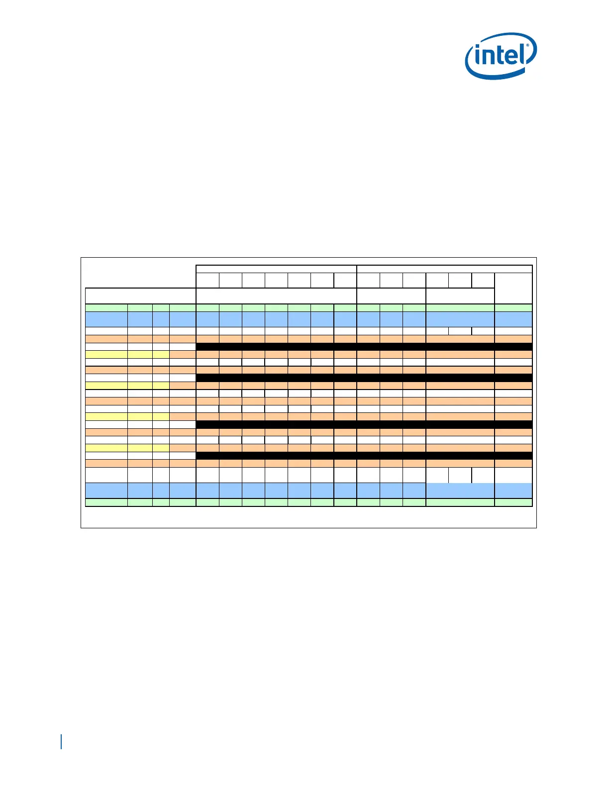
3.2 Platform Stack-Up
Figure 4 shows the recommended platform stack-up.
Signal layers are dual referenced asymmetric stripline on layers 3, 5, 6, and 8 and
microstrip on layers 1 and 10. Signal layers 1, 3, 5, 6, 8, and 10 are referenced to
ground.
Intel strongly recommends that system designers use the stack-up shown in Figure 4
and recommendations in Table 7 when designing their boards. Intel realizes numerous
ways exist to achieve these targeted impedance tolerances; contact your board vendor
for these specifics. Intel encourages platform designers to perform comprehensive
simulation analysis to ensure all timing specifications are met. This is particularly
important if a design deviates from the provided design guidelines.
General Routing Guidelines
• All length and matching rules assume pin to pin unless otherwise noted.
• Microstrip or stripline routing is assumed for each interface unless otherwise noted.
• Minimize the number of vias used for each interface.
• Never route signals over plane splits and always try to maintain the same reference
plane.
• Avoid 90° bends.
• Although there is a large core thickness between layers 5 & 6, try to minimize the
length that traces run parallel on adjacent layers.
• Do not route critical signals under inductors or other noisy components.
Figure 4. PCB Recommended 10-Layer Stack-Up
ohms
ohms
ohms
ohms
ohm
ohms
ohms
ohms
ohms
ohm
ohms
ohms
ohms
Thk.
(mils)
Er
Soldermask 0.8 3.60
Copper Plate 1.3
Copper Foil 0.6 L1 Top 3.75 4.50 5.50 6.25 6.75 8.50 15.50 4.00 4.75 6.00 10.00 10.00 12.00 L2
Pre-preg 3.6 4.11
1.2 L2 Pln
Core 4 4.10
0.6 L3 Sig 3.75 4.50 4.75 5.50 6.50 11.50 3.75 4.50 5.50 10.00 10.00 13.00 L2/L4
Pre-preg 6 4.10
1.2 L4 Pln
Core 4 4.10
0.6 L5 Sig 4.25 5.00 6.00 6.50 7.25 9.00 16.00 4.25 5.00 6.00 10.00 10.00 11.00 L4/L7
Pre-preg 25 4.10
0.6 L6 Sig 4.25 5.00 6.00 6.50 7.25 9.00 16.00 4.25 5.00 6.00 10.00 10.00 11.00 L4/L7
Core 4 4.10
1.2 L7 Pln
Pre-preg 6 4.10
0.6 L8 Sig 3.75 4.50 4.75 5.50 6.50 11.50 3.75 4.50 5.50 10.00 10.00 13.00 L7/L9
Core 4 4.10
1.2 L9 Pln
Pre-preg 3.6 4.11
Copper Foil 0.6 L10 Bot 3.75 4.50 5.50 6.25 6.75 8.50 15.50 4.00 4.75 6.00 10.00 10.00 12.00 L9
Copper Plate 1.3
Soldermask 0.8 3.60
72.80 *Finished board thickness (After plating and solder mask):
Sin
le-ended Ed
e-coupled differentia
Reference
Plane
Finished Trace Width (mils)
Finished Trace Width
(mils)
Trace to Trace
Centers (mils)