Intel
®
EP80579 Integrated Processor Product Line May 2010
Order Number: 320068-005US 342
System Memory Interface (Memory Down)—Intel
®
EP80579 Integrated Processor Product Line
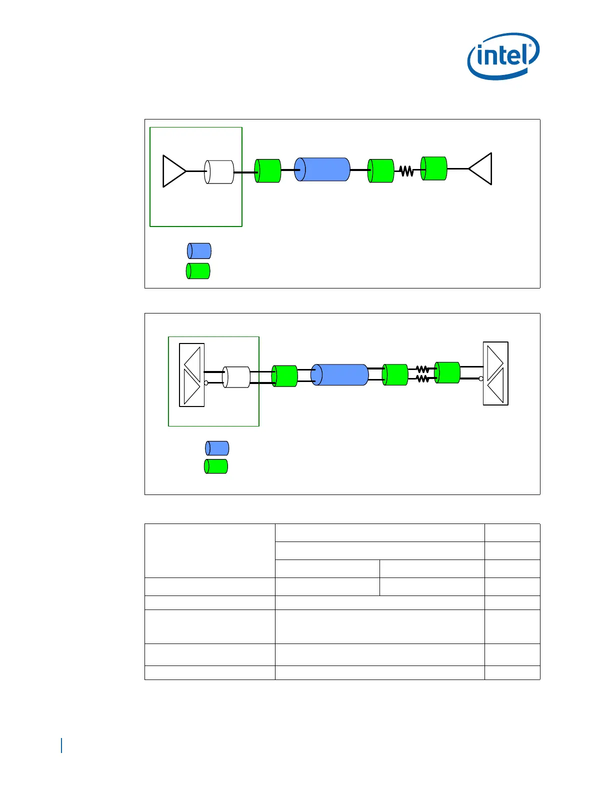
Figure B-10. DDR2 Data/DM/ECC Byte Lane Topology
Figure B-11. DDR2 Data Strobe Routing (DQS/DQS#) Topology (One Strobe per Byte Lane)
Table B-29. Data and Strobe Signal Group Routing Guidelines (Sheet 1 of 2)
Parameter
Routing Guidelines Figure
Data Byte Lane
Data & Data Mask Strobe
Signal Group Data & Mask (DQ & DM)
Byte Strobe (DQS/DQS#)
Reference Plane Ground Referenced
Characteristic Trace Impedance
(Zo)
Single Ended Impedance
•50Ω ±10% for L1/L10 (Microstrip routing (e2e))
•45Ω ±10% for L3/L5/L6/L8 (Stripline routing (e2e))
Layer assignment
• Signals within the same Byte Lane must be routed on
the same layer
Nominal Trace Width See Stackup
Pkg
=
Microstrip Routing
=
Stripline Routing
SDRAM
Rsd
L2L0
EP80579
L1
Lp
L3
Pkg
=
Microstrip Routing
=
Stripline/Microstrip Routing
SDRAM
Rsd
L2
L0
EP80579
Lp
L3
L1