Intel
®
EP80579 Integrated Processor Product Line—Platform System Clock
Intel
®
EP80579 Integrated Processor Product Line
Platform Design Guide May 2010
101 Order Number: 320068-005US
8.2.3.1 Sharing 33 MHz Clocks
In some cases, the designer may have a need to share one 33 MHz clock between two
down devices (this is not implemented on the development platform). In this case, the
driver is the clock synthesizer 33 MHz clock output buffer and the receivers are the
33 MHz clock input buffers of two separate down devices.
8.2.4 CLK14 Group
The driver in the CLK14 group is the clock synthesizer 14.318 MHz clock output buffer
and the receiver is the 14.318 MHz clock input buffer at the EP80579 and SIO.
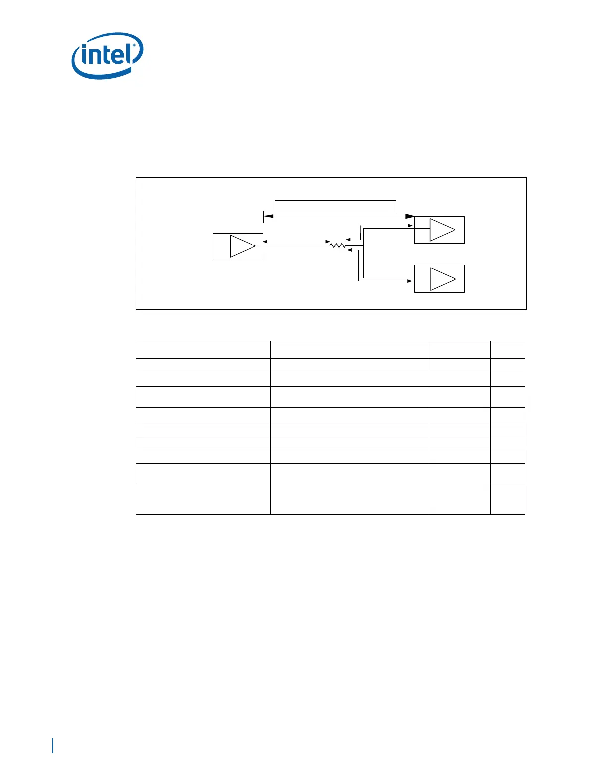
Figure 61. Topology for Sharing CLK33 Between Two Down Devices
Table 22. CLK33 Routing Guidelines for Two Down Devices
Parameters Routing Guidelines Illustrations Notes
Clock Group CLK33: 33 MHz clock
Topology Balanced T Topology Figure 61
Reference Plane Ground referenced (contiguous over entire
length)
1
Characteristic Trace Impedance (Z
0
) 55 Ω ± 10%
Trace Width (W) 4.5 mils (Target Z
0
first) Figure 60
Trace Spacing (S1) 20 mils Figure 60
Resistor Rs = 12 Ω
±5% Figure 61 2
Clk Driver to Rs for PCI Down
Devices (L1)
0.5” max
Figure 61
Rs to Down Device (L2) L2 = [Z + (0” to 6”)] = 20” max. L2
lengths should be matched to within 250
mils of each other.
Figure 61 3
Notes:
1. Ground referencing is preferred. However CLK33 can be routed referenced to other planes assuming
that the plane is contiguous from source to destination.
2. The value of Rs may need to be increased for shorter trace lengths to minimize overshoot /
undershoot effects.
3. Length “Z” is the distance from the 33 MHz clock driver to the EP80579 33 MHz input buffer. “Z” can
be 2
” to 20” long.
L1
L2
L2
Clock
Driver
Rs
LT=L1+L2
Down device
Down device