Intel
®
EP80579 Integrated Processor Product Line—Universal Serial Bus (USB) Interface
Intel
®
EP80579 Integrated Processor Product Line
Platform Design Guide May 2010
172 Order Number: 320068-005US
Common mode chokes distort full-speed and high-speed signal quality. As the common
mode impedance increases, the distortion will increase, so you must test the effects of
the common mode choke on full-speed and high-speed signal quality. Common mode
chokes with a target impedance of 80–90 Ω at 100 MHz generally provide adequate
noise attenuation.
Finding a common mode choke that meets the designer’s needs is a two-step process:
• Choose a part with the impedance value that provides the required noise
attenuation. This is a function of the electrical and mechanical characteristics of the
part chosen and the frequency and strength of the noise present on the USB traces
that must be suppressed.
• After obtaining a part that gives passing EMI results, the second step is to test the
effect this part has on signal quality. Higher impedance common mode chokes
generally have a greater damaging effect on signal quality, so use care when
increasing the impedance without doing thorough testing. Thorough testing means
that the signal quality must be checked for low-speed, full-speed, and high-speed
USB operation.
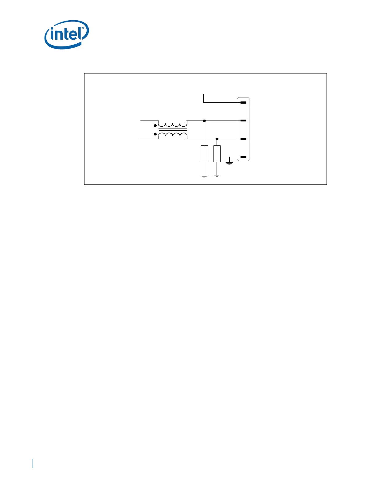
12.6 ESD
Classic USB (1.0/1.1) provided ESD suppression by using in-line ferrites and capacitors
that formed a low pass filter. This technique doesn’t work for USB 2.0 because of the
higher signal rate of high-speed data. A device that has been tested successfully is
based on spark gap technology. Proper placement of any ESD protection device is on
the data lines between the common mode choke and the USB connector data pins as
shown in Figure 116. Other types of low-capacitance ESD protection devices may work
as well, but were not investigated. As with the common mode choke solution, Intel
recommends designers include footprints for some type of ESD protection device as a
stuffing option in case it is needed to pass ESD testing.
Recommended proper placement of any ESD protection device is "on the data lines
between the common mode choke and the USB connector signal pin". Constraints to
control these placements are not included in this rule set. Stubs caused by these
components must be less than 0.200".
Figure 116. A Common Mode Choke
Vcc
USB A
Connector
D+
D-
ESD Supression
Components
Common Mode
Choke