Intel
®
EP80579 Integrated Processor Product Line May 2010
Order Number: 320068-005US 94
Platform System Clock—Intel
®
EP80579 Integrated Processor Product Line
8.2 System Clock Groups
Each of the clock groups mentioned in Table 16 are discussed in the following sections.
8.2.1 HOST_CLK Group
The clock synthesizer provides three sets of 100/133 MHz differential clock outputs.
Two of the differential clocks are driven to EP80579 (CLKP100/CLKN100), and to the
ITP Debug Port (BCLKP/BCLKN), as shown in Figure 52 . The HOST_CLK Group
Topology and Routing guidelines provided in this section applies to the routing of the
differential clocks from the clock synthesizer to EP80579 or to the ITP Debug Port
The clock driver differential bus output structure is a “current mode current steering”
output, which develops a clock signal by alternately steering a programmable constant
current to the external termination resistors, designated as Rt. The resulting amplitude
is determined by multiplying IOUT by the value of Rt. The current IOUT is
programmable by a resistor and an internal multiplication factor, so the amplitude of
the clock signal can be adjusted for different values of resistance to match impedances
or to accommodate future load requirements. See the CK410B Clock Synthesizer/
Driver Specification for more information.
8.2.1.1 HOST_CLK Topology
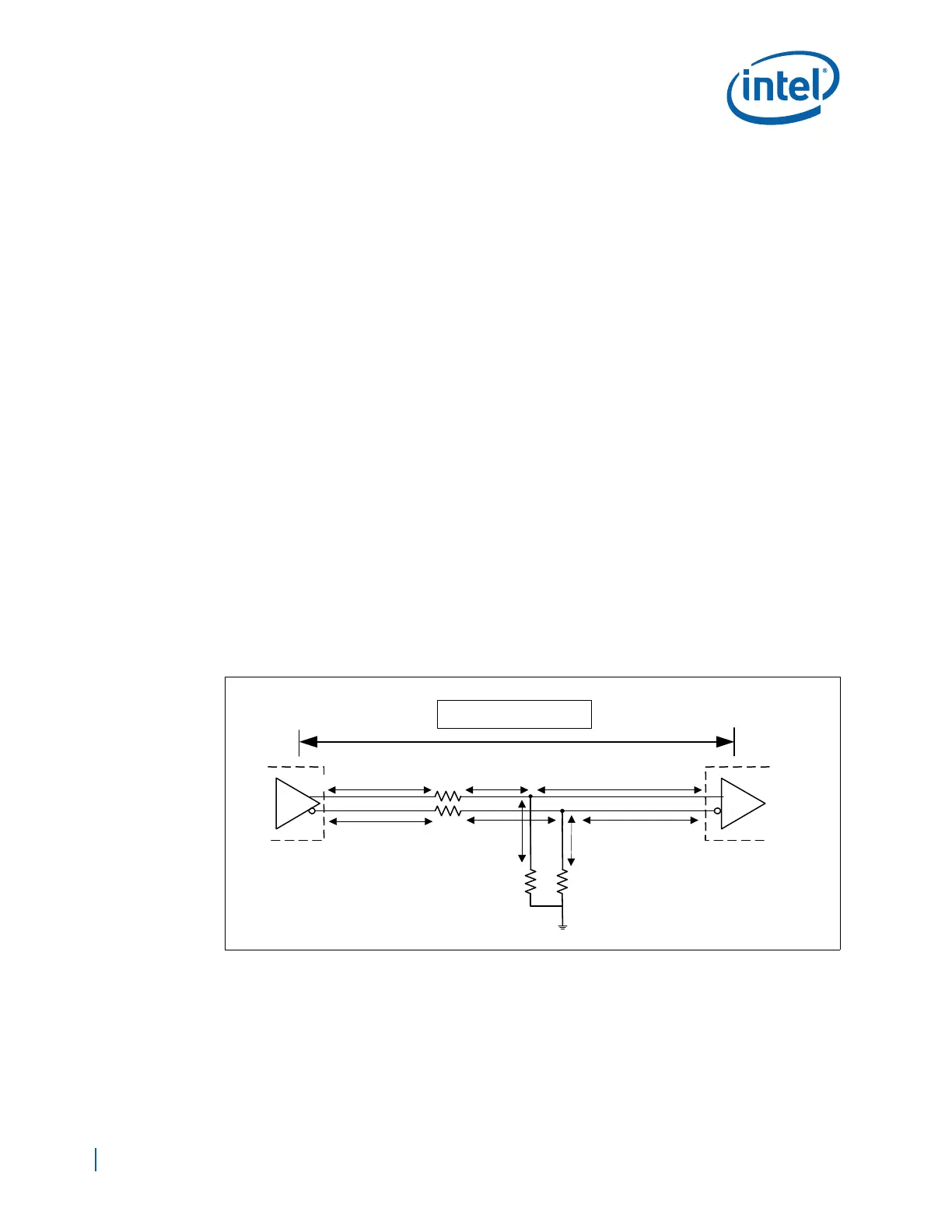
The recommended termination for the differential bus clock is a “shunt source
termination.” See Figure 53 for an illustration of this terminology scheme. Parallel Rt
resistors perform a dual function, converting the current output of the clock driver to a
voltage and matching the driver output impedance to the transmission line. The series
resistors, designated as Rs, provide isolation from the clock driver's output parasitics,
which would otherwise appear in parallel with Rt.
Select a value for Rt to match the characteristic impedance of the baseboard.
Figure 53. Source Shunt Termination
L1
Rs
L2
L2'
L3
L3'
L4
L4'
Clock
Driver
EP80579
Rs
Rt Rt
LT = L1 + L2 + L4
L1'