Intel
®
EP80579 Integrated Processor Product Line May 2010
Order Number: 320068-005US 140
PCI Express* Interface—Intel
®
EP80579 Integrated Processor Product Line
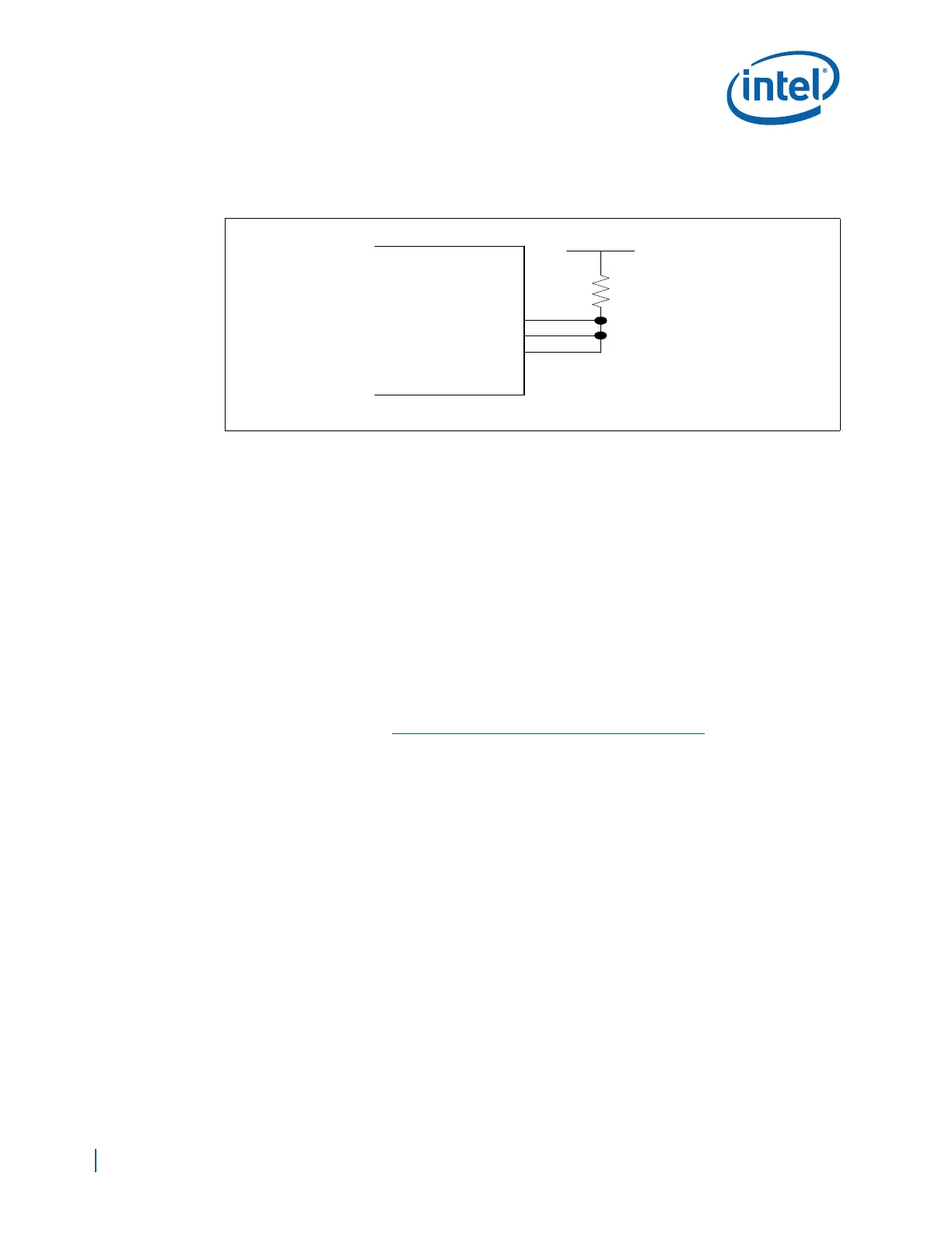
10.1.5 Compensation Resistor Signals Guidelines
The PCI Express interface has three compensation resistors on the PCI Express port.
The following signals are used to calibrate the PCI Express high-speed serial input/
output buffers:
•PEA_RCOMPO
•PEA_ICOMPI
•PEA_ICOMPO
The PEA_RCOMPO, PEA_ICOMPI and PEA_ICOMPO signals must be tied directly to each
other at the EP80579 and terminate to VCCPE (1.2V) through a 24.9Ω ±1% resistor, as
shown in Figure 89.
10.1.6 PCI Express Clocks Routing Guidelines
PEA_CLKp, and PEA_CLKn are the differential clock pairs for the PCI Express port.
These clocks are inputs to the EP80579 and used to derive the internal clock. These
clocks are not used for PCI Express devices. Detailed routing information for these
signals can be found in Section 8.2.2, “CLK100 (SRC Clock) Group”
.
10.1.7 Topology 1 – EP80579 to PCI Express Connector
Table 49 and Figure 90 summarize the layout routing solution space to a PCI Express
connector. In this case, the EP80579 is a transmitter and the PCI Express connector is a
receiver. L1, L2, and L3 must be routed on the same layer.
• L1 starts from the EP80579 breakout region to the AC blocking capacitor via.
• L2 is the main routing section that is from the AC blocking capacitor via to the PCI
Express connector breakout region.
• L3 is the breakout region of the PCI Express connector.
• LT is the main routing section that is from the EP80579 pin to the PCI Express
connector.
Figure 89. PCI Express Compensation Signal Guidelines
PEA _ICOMPI
EP80579
PEA_RCOM PO
VCCPE (1.2V)
24.9±1%
Ω
PEA _ICOM PO