Intel
®
EP80579 Integrated Processor Product Line May 2010
Order Number: 320068-005US 325
System Memory Interface (SODIMM)—Intel
®
EP80579 Integrated Processor Product Line
A.4.5.3 DDR2 Control Signals – DDR_CS[1:0]#, DDR_ODT[1:0],
DDR_CKE[1:0]
In the EP80579 memory configuration, the DDR_CKE, DDR_ODT, and DDR_CS# signals
make up the control signal group. EP80579 provides six signals: DDR_CS[1:0]#,
DDR_ODT[1:0], and DDR_CKE[1:0] as control signals for two-rank memory support.
On the SODIMM, one chip select signal, one ODT control line, and one clock enable
signal are required for each rank. Figure A-4 provides the inter-connect implementation
of the control signals to the SODIMM.
A.4.5.3.1 ODT Settings
Table A-8 and Table A-9 provides the DDR2 Controller and SODIMM ODT settings for
write and read operations to/from single-rank and dual-rank SODIMM modules.
Inter-pair Trace Spacing(e2e)
(CLK to CLK# spacing)
6.0 mils Figure A-3
Pair-to-Pair Spacing (e2e) 20.0 mils
Clearance from other signals groups 20.0 mils Figure A-3
Board Routing Guidelines
Total Trace Length (TTL) = (L
PKG
+
L
BREAKOUT
+ L
ROUTE
)
1.0 in - 5.0 in
L
PKG
See the Intel
®
EP80579 Integrated Processor Product Line Datasheet
for package length information.
L
BREAKOUT
Max = 0.8 in
L
ROUTE
Max = 4.0 in
Length/Skew Matching Rules
• The clock differential pairs need to match in
length within ± 10 mils (CLK[x] = CLK[x]# ±
10 mils, x= 0.. 1)
• Clock pairs should be matched in length to other
clock pairs within ± 20 mils
• Clock signals should be matched in length to
CMD/ADD within ± 20 mils. (CLK/CLK# = CMD/
ADD ± 20 mils)
Table A-7. Clock Signal Group Routing Guidelines (Sheet 2 of 2)
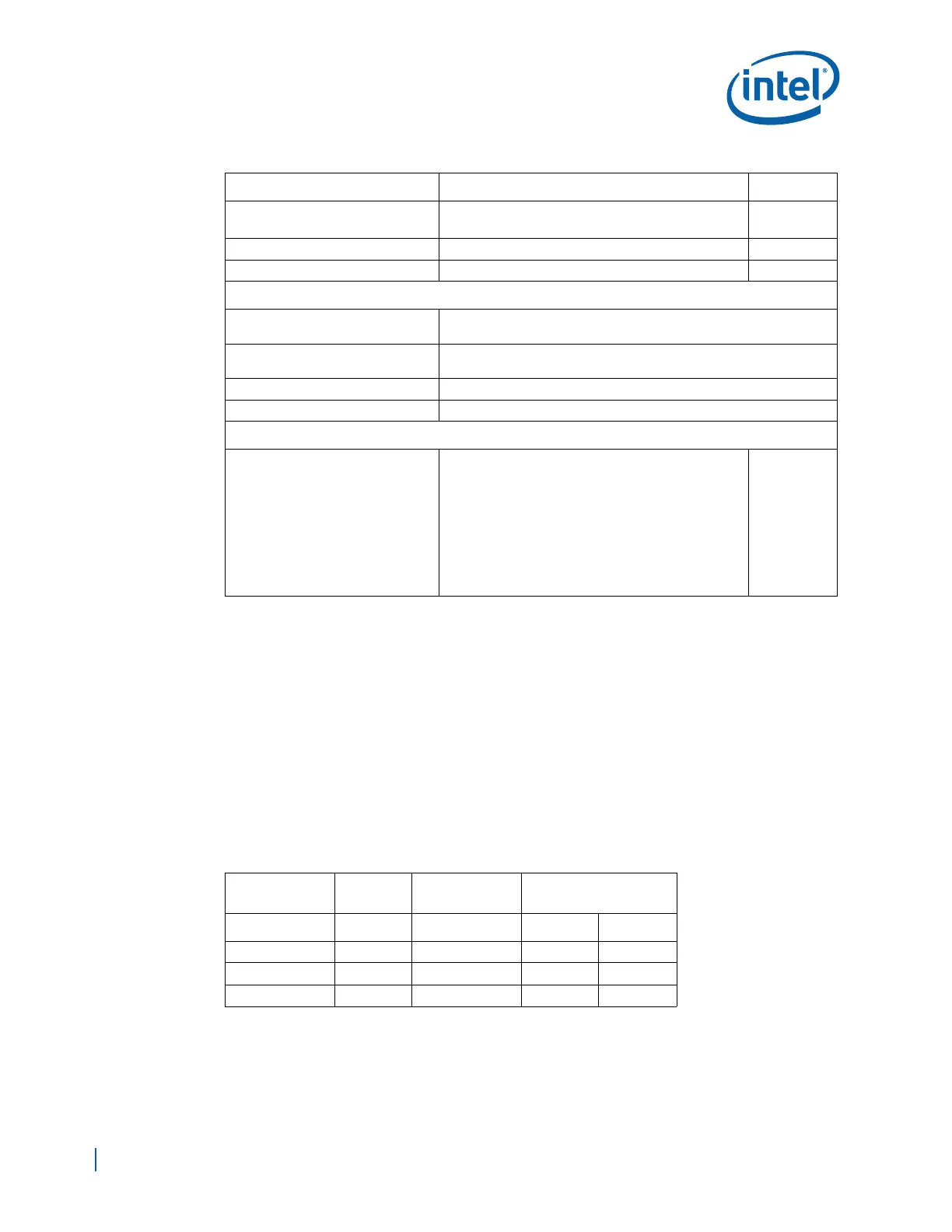
Parameter Routing Guidelines for SODIMM Figure
Table A-8. Write Operation ODT Table
SODIMM
Module
Write
Target
Controller
Configuration
SODIMM
Configuration
Rank0 Rank1
1-Rank (SR) Rank0 ODT Off ODT Off n/a
2-Rank (DR) Rank0 ODT Off ODT Off 150 Ω
2-Rank (DR) Rank1 ODT Off 150 Ω ODT Off

 Loading...


