Intel
®
EP80579 Integrated Processor Product Line May 2010
Order Number: 320068-005US 323
System Memory Interface (SODIMM)—Intel
®
EP80579 Integrated Processor Product Line
Board Routing Guidelines
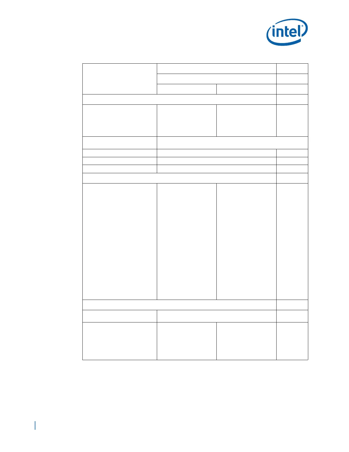
Total Trace Length (TTL) = (L
PKG
+
L
BREAKOUT
+ L
ROUTE
+ L
BREAKIN
)
2.0 in - 5.0 in
• Min TTL (DQS/DQS#)
= Min TTL (DQ/DM) -
200 mils
• Max TTL (DQS/DQS#)
= Max TTL (DQ/DM) -
200 mils
Figure A-2
L
PKG
See the Intel
®
EP80579 Integrated Processor Product Line Datasheet for
package length information.
L
BREAKOUT
B = 0.8 in (max)
L
ROUTE
C = 1.0 in - 4.0 in
L
BREAKIN
D = 0.8 in (max)
Length/Skew Matching Rules
Length Tuning Requirements
• Only length matching
is required within each
Byte lane. No signal
length matching is
required outside the
Byte lane. For
example, any signal
within Data Byte Lane
0 (DQ [0...7]) need not
be length matched to
DQS1
•DQ/DM should match
each other to 20 mils
or less within the same
byte lane.
• The trace length
difference between
DQS and DQS# should
not be more than 10
mils. - that is,
DQS[x] =
DQS[x]#±10 mils, x = 0..
7
• Length match the data
strobes (DQS/DQS#)
to the associated data
mask and data (DQ/
DM) signals for each
Data Byte Lane:
• Min TTL (DQS/DQS#)
= Min TTL (DQ/DM) -
200 mils
• Max TTL (DQS/DQS#)
= Max TTL (DQ/DM) -
200 mils
Routing Rules
Layer Routing Requirements
Signals within a data byte lane must be routed on the
same layer.
DQS-to-Clock
Length match Strobe
(DQS/DQS#) to Clock
(CLK/CLK#) to within
500 mils:
• DQS/DQS# = CLK/
CLK# ± 500 mils
Table A-6. Data and Strobe Signal Group Routing Guidelines (Sheet 2 of 2)
Parameter
Routing Guidelines Figure
Data Byte Lane
Data & Data Mask Strobe

 Loading...


