GD32F3x0 User Manual
543
20.5. Register definition
SPI0/I2S0 base address: 0x4001 3000
SPI1 base address: 0x4000 3800
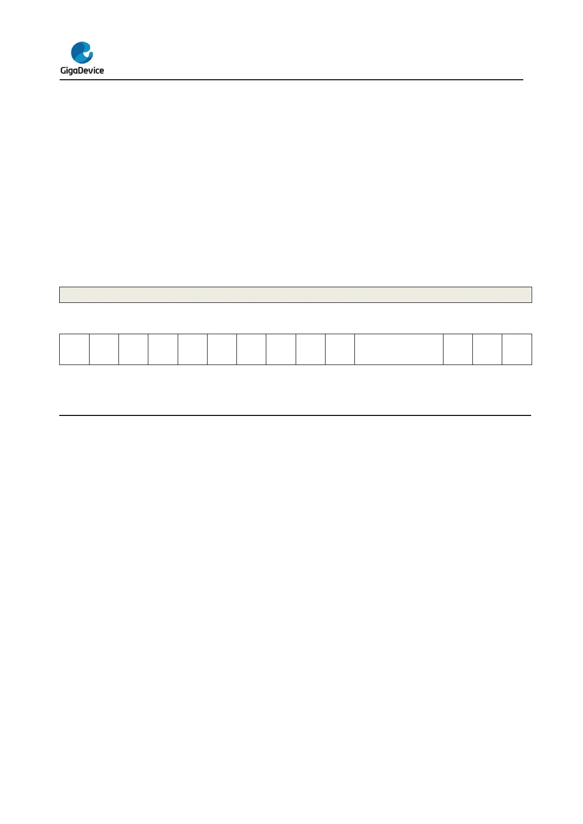
20.5.1. Control register 0 (SPI_CTL0)
Address offset: 0x00
Reset value: 0x0000 0000
This register can be accessed by byte (8-bit) or half-word (16-bit) or word (32-bit).
This register has no meaning in I2S mode.
Must be kept at reset value.
Bidirectional enable
0: 2 line unidirectional transmit mode
1: 1 line bidirectional transmit mode. The data transfers between the MOSI pin of
master and the MISO pin of slave.
Bidirectional transmit output enable
When BDEN is set, this bit determines the direction of transfer.
0: Work in receive-only mode
1: Work in transmit-only mode
CRC calculation enable
0: Disable CRC calculation.
1: Enable CRC calculation.
CRC next transfer
0: Next transfer is data
1: Next transfer is CRC value
When the transfer is managed by DMA, CRC value is transferred by hardware.
This bit should be cleared.
In full-duplex or transmit-only mode, set this bit after the last data is written to
SPI_DATA register. In receive only mode, set this bit after the second last data is


 To Next Page