Intel
®
EP80579 Integrated Processor Product Line—Gigabit Ethernet (GbE) Interface
Intel
®
EP80579 Integrated Processor Product Line
Platform Design Guide May 2010
213 Order Number: 320068-005US
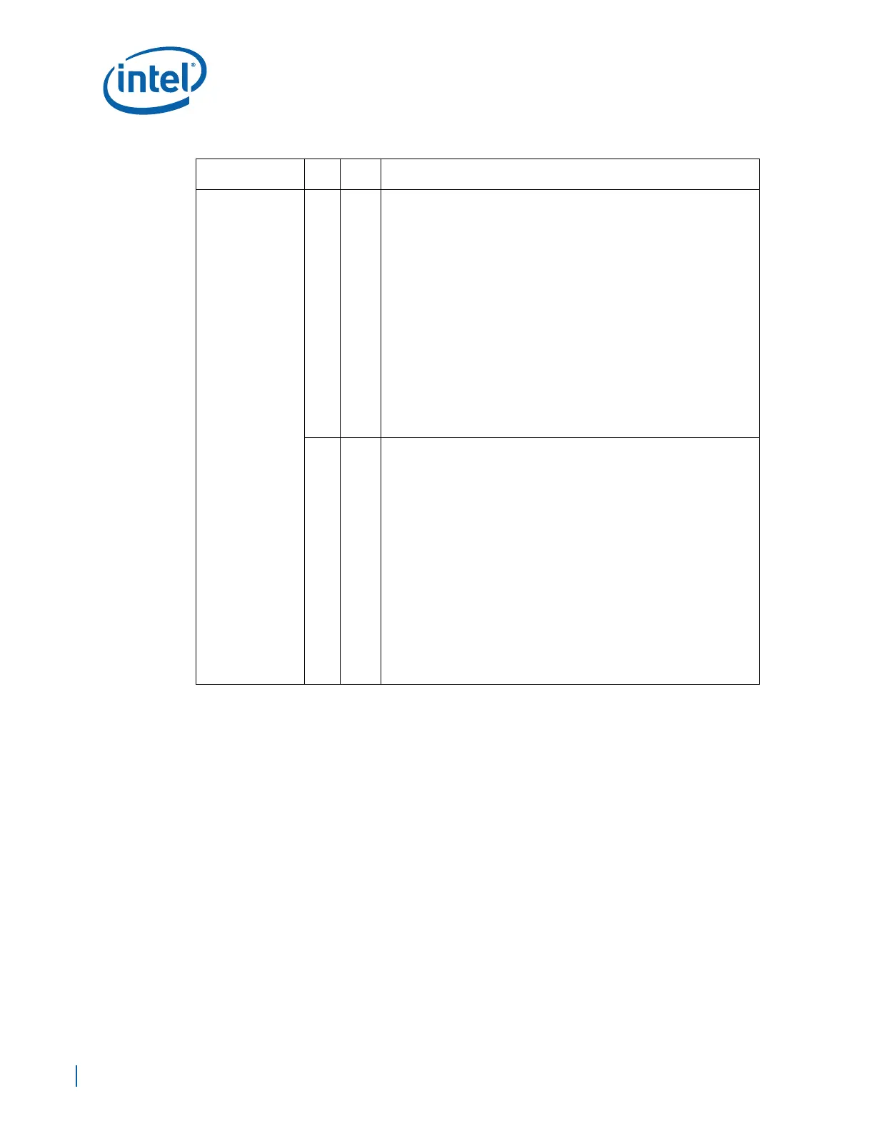
GBEn_RxCTL
I1
RGMII Mode of Operation:
• The signal name is GBEn_RxCTL and connected to the PHY RX_DV
when operating in RGMII mode of operation.
• GBEn_RxCTL (PHY RX_DV) is driven by the PHY to indicate that the
PHY is presenting recovered and decoded data on the
GBEn_RXDATA[3:0] bundle. GBEn_RxCTL transitions synchronously
with respect to the GBEn_RxCLK. GBEn_RxCTL shall be asserted
continuously from the first recovered nibble of the frame through the
final recovered nibble and shall be negated prior to the first rising edge
of GBEn_RxCLK that follows the final nibble. In order for a received
frame to be correctly interpreted by the MAC and the MAC sublayer,
GBEn_RxCTL must encompass the frame, starting no later than the
Start Frame Delimiter (SFD) and excluding any End-of-Frame
delimiter.
• Pull up GBE Port 0 Receive Control signal to EP80579 2.5V Standby
Voltage (VCCSUS25) using a 1.2KΩ ± 5% resistor.
• Pull up GBE Port 1&2 Receive Control signals to GBE 2.5V using a 1.2KΩ
± 5% resistors.
• Pull-down all unused Receive Control signals to GND using 10 KΩ
resistors.
I1
RMII Mode of Operation:
• The signal name is GBEn_RxCTL and connected to the PHY CRS_DV
when operating in RMII mode of operation.
• GBEn_RxCTL (PHY CRS_DV) shall be asserted by the PHY when the
receive medium is non-idle. Loss of carrier shall result in the
deassertion of GBEn_RxCTL synchronous to the cycle of REF_CLK
which presents the first two-bits of a nibble onto GBEn_RxDATA[1:0]
(i.e. GBEn_RxCTL is deasserted only on nibble boundaries). During a
false carrier event, GBEn_RxCTL shall remain asserted for the duration
of carrier activity. The data on GBEn_RxDATA[1:0] is considered valid
once GBEn_RxCTL is asserted. However, since the assertion of
GBEn_RxCTL is asynchronous relative to REFCLK, the data on
GBEn_RxDATA[1:0] shall be “00” until proper receive signal decoding
takes place.
• Pull up GBE Port 0 Receive Control signal to EP80579 3.3V Standby
Voltage (VCCGBEPSUS) using a 1.2KΩ ± 5% resistor.
• Pull up GBE Port 1&2 Receive Control signals to GBE 3.3V using a 1.2KΩ
± 5% resistors.
• Pull-down all unused Receive Control signals to GND using 10 KΩ
resistors.
Table 80. GBEn Pin Table (Sheet 3 of 4)
GBEn Signal Name
Pin
Type
Pin
Count
Description

 Loading...


