Register Model
PowerPC e500 Core Family Reference Manual, Rev. 1
Freescale Semiconductor 2-43
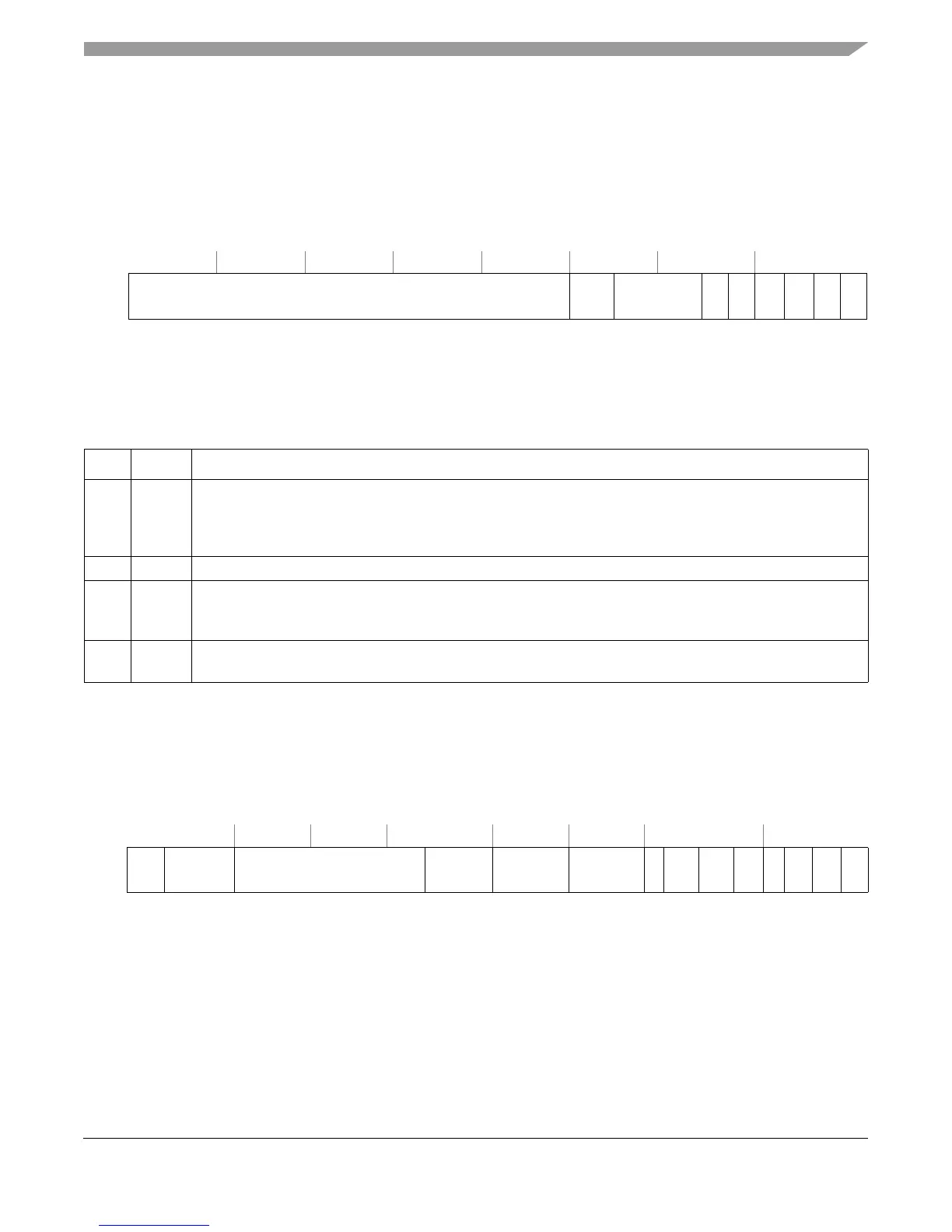
2.12.5.4 MAS Register 3 (MAS3)
Figure 2-32 shows the format of MAS3. Writing to MAS3 requires synchronization, as described
in Section 2.16, “Synchronization Requirements for SPRs.”The core complex uses the same bit
definitions as the Freescale Book E standard for MAS3 for 32-bit implementations.
The MAS3 fields are described in Table 2-27.
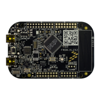
2.12.5.5 MAS Register 4 (MAS4)
Figure 2-33 shows the format of MAS4. Writing to MAS4 requires synchronization, as described
in Section 2.16, “Synchronization Requirements for SPRs.”
SPR 627 Access: Supervisor-only
32 51 52 53 54 57 58 59 60 61 62 63
R
RPN — U0–U3 UX SX UW SW UR SR
W
Reset All zeros
Figure 2-32. MAS Register 3 (MAS3)
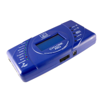
Table 2-27. MAS3 Field Descriptions—RPN and Access Control
Bits Name Description
32–51 RPN Real page number. Depending on page size, only the bits associated with a page boundary are valid. Bits that
represent offsets within a page are ignored and should be zero. Note that, on the e500v2, additional bits of the
RPN are contained in MAS7. See Section 2.12.5.7, “MAS Register 7 (MAS7)—e500v2 Only,” for more
information.
52–53 — Reserved, should be cleared.
54–57 U0–U3 User attribute bits. These bits are associated with a TLB entry and can be used by system software. For
example, these bits may be used to hold information useful to a page scanning algorithm or be used to mark
more abstract page attributes.
58–63 PERMIS Permission bits (UX, SX, UW, SW, UR, SR). User and supervisor read, write, and execute permission bits. See
the
EREF
for more information on the page permission bits as they are defined by Book E.
SPR 628 Access: Supervisor-only
32 33 34 35 36 45 46 47 48 55 56 57 58 59 60 61 62 63
R
— TLBSELD — TIDSELD — TSIZED — X0D X1D WD ID MD GD ED
W
Reset All zeros
Figure 2-33. MAS Register 4 (MAS4)