Register Model
PowerPC e500 Core Family Reference Manual, Rev. 1
Freescale Semiconductor 2-31
2.11 L1 Cache Configuration Registers
The Freescale Book E standards define registers that provide control and configuration and status
information for the L1 cache implementation.
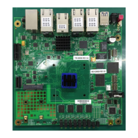
2.11.1 L1 Cache Control and Status Register 0 (L1CSR0)
The L1CSR0 register, shown in Figure 2-20, is defined by the EIS. It is used for general control
and status of the L1 data cache. Writing to L1CSR0 requires synchronization, as described in
Section 2.16, “Synchronization Requirements for SPRs.”
51 ABE Address broadcast enable. The e500 broadcasts cache management instructions (dcbst, dcblc (CT = 1),
icblc (CT = 1), dcbf, mbar, msync, tlbivax, tlbsync, icbi) based on ABE. On some implementations, ABE
must be set to allow management of external L2 caches.
0 Address broadcasting disabled
1 Address broadcasting enabled
52 — Reserved, should be cleared.
53 MPXTT MPX re-map transfer type
0 TTx codes are not remapped.
1 Certain TTx codes are remapped for MPX bus compatibility. See the integrated device documentation.
54–55 — Reserved. should be cleared.
56 ATS Atomic status (read-only). Indicates state of atomic status bit in bus unit.
57–59 — Reserved, should be cleared.
60–63 MID Reflected directly from the MID input pins (read-only)
SPR 1010 Access: Supervisor-only
Line Locking APU Bits
32 46 47 48 49 51 52 53 54 55 56 61 62 63
R
— CPE CPI — CSLC CUL CLO CLFR — CFI CE
W
Reset All zeros
Figure 2-20. L1 Cache Control and Status Register 0 (L1CSR0)
Table 2-15. HID1 Field Descriptions (continued)
Bits Name Description