Endian Control (Byte and Word Swapping)BCM5718 Programmer’s Guide
Broadcom®
January 29, 2016 • 5718-PG108-R Page 197
Word Swap Data and Byte Swap Data Bits
The Word Swap Data, and Byte Swap Data bits effect how packet data is ordered on the PCI bus. These only
affect how packet data is ordered, and do not affect non-frame data (i.e., buffer descriptors, statistics block, etc.).
In other words, these bits effect how data is transferred to/from host send/receive buffers.
Example: If Ethernet controller were to receive a packet that had the following byte order:
Where:
• D1–D6 consists of the packet’s destination address (Byte D0 is the first byte on the wire);
• S1–S6 is the source address;
• T1–T2 is the Ethernet type/length field;
• IP1–IP2 are the first two bytes of the IP header which immediately follow the type/length field.
The packet would be stored internally in big endian format:
However, when the data gets transferred across PCI, there could be confusion about the correct byte ordering
because PCI is Little Endian whereas Ethernet controller is a Big Endian device. So, in order to provide flexibility
for different host processor/memory architectures, Ethernet controller can order this data on PCI in four different
ways depending on the settings of the Word Swap Data, and Byte Swap Data bits. The following figures illustrate
how data would appear on the PCI AD[63:0] pins depending on the settings of those swap bits:
Word Swap Data = 0, and Byte Swap Data = 0
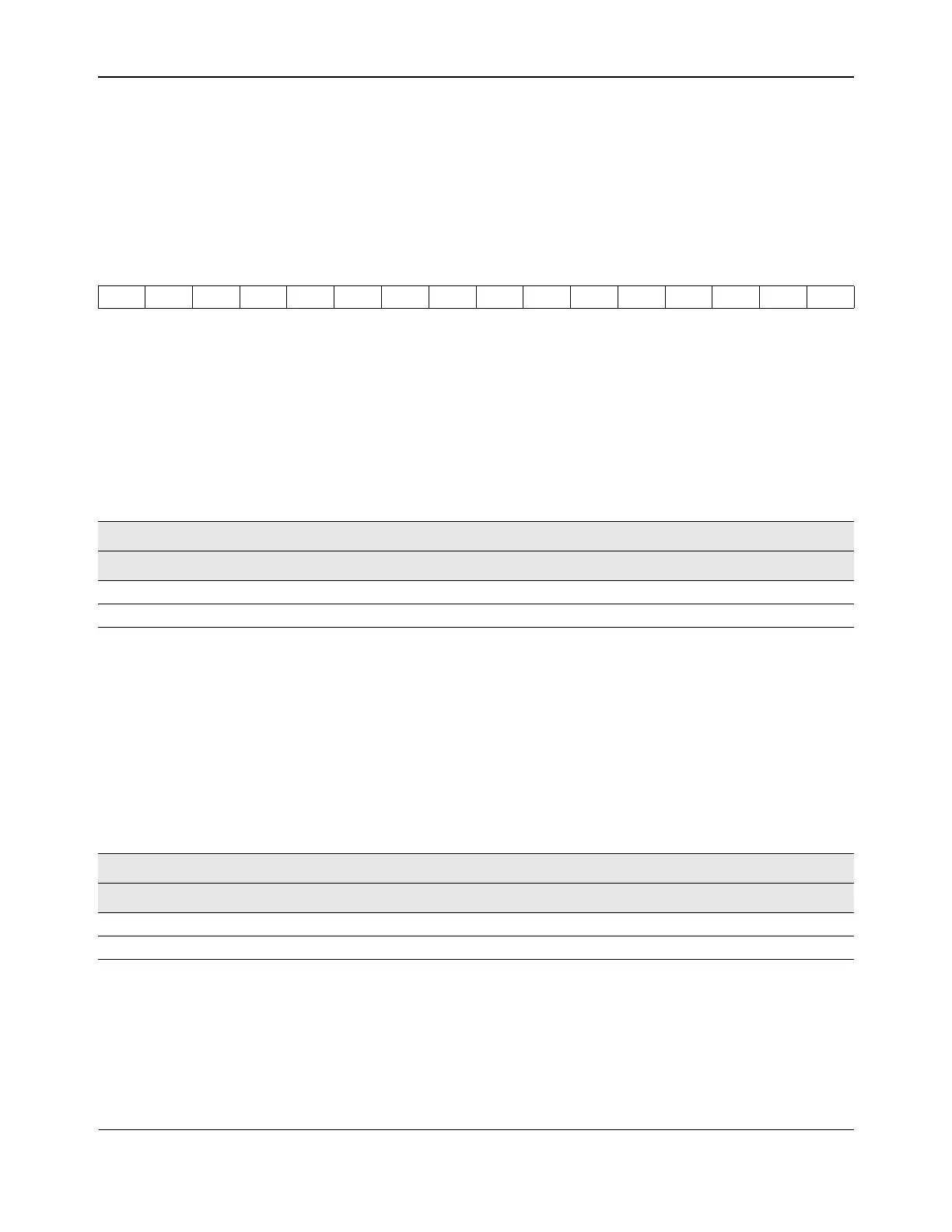
01 02 03 04 05 06 07 08 09 0A 0B 0C 0D 0E 0F 10
D1 D2 D3 D4 D5 D6 S1 S2 S3 S4 S5 S6 T1 T2 IP1 IP2
Table 59: Big-Endian Internal Packet Data Format
B0 B1 B2 B3 B4 B5 B6 B7
63–56 55–48 47–40 39–32 31–24 23–16 15–8 7–0
D1 D2 D3 D4 D5 D6 S1 S2
S3 S4 S5 S6 T1 T2 IP1 IP2
Table 60: 64-Bit PCI Bus (WSD = 0, BSD = 0)
B7 7B6 B5 B4 B3 B2 B1 B0
63–56 55–48 47–40 39–32 31–24 23–16 15–8 7–0
D1 D2 D3 D4 D5 D6 S1 S2
S3 S4 S5 S6 T1 T2 IP1 IP2
 Loading...