10h–1Fh Register Map Detailed DescriptionBCM5718 Programmer’s Guide
Broadcom®
January 29, 2016 • 5718-PG108-R Page 525
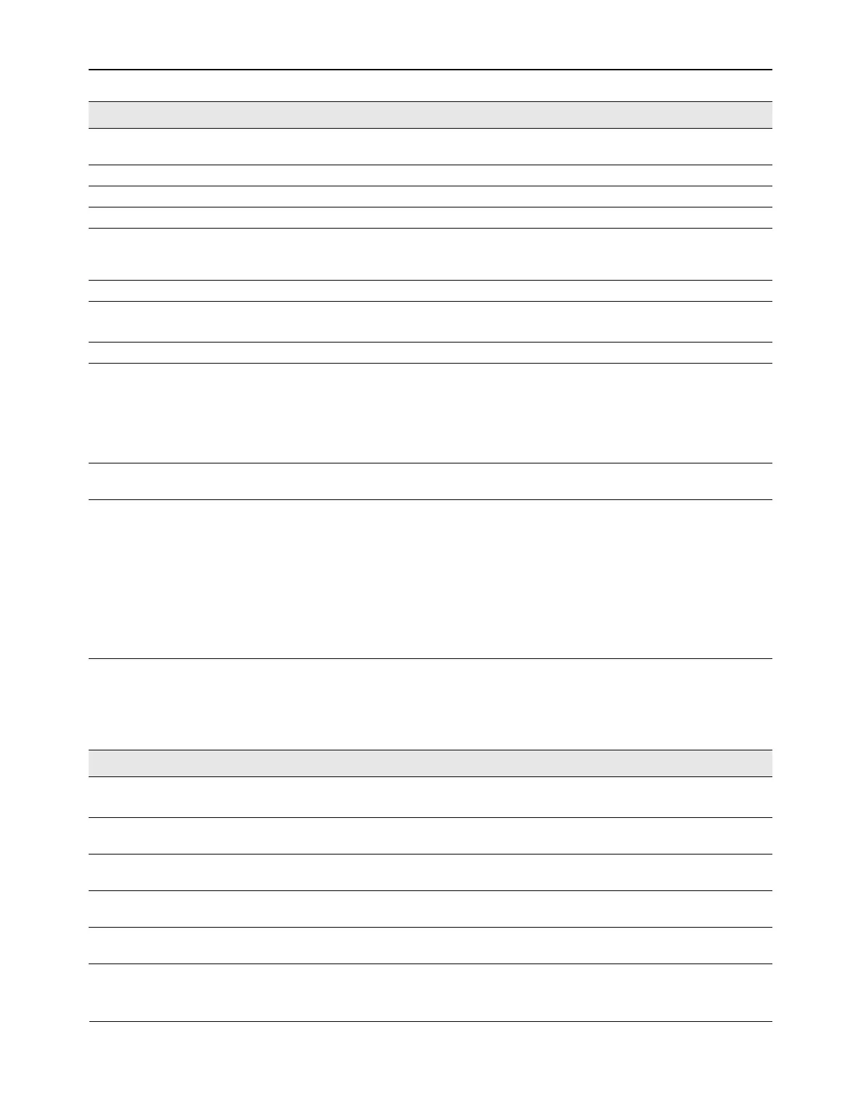
1Ch: Clock Alignment Control Register (Shadow Register Selector =
“03h”)
14:10 SHADOW REGISTER
SELECTOR
RW Shadow Register Selector 00010
9 SD status RO 1= sd input active 0
8 FORCE SD ON RW 1= force sd on. disable sd pin input 0
7 INVERT SD PIN RW 1 = invert sd pin 0
6 CFC_INITFILTER
ENABLE
RW 1 = enable cfc_initFilter signal to control clock
gating of 1000t clocks. Do not gate off 1000t
clocks wherever cfiltercntl is initializing the filter.
0
5 USE FILTERED SD RW 1= enable filter on sd input pin 0
4 100FX MODE COPPER
PATH
RW 1 = enable 100BASE-FX on TRD+/- pins
0 = normal copper operation on MDI pairs
0
3 RESERVED RW write as 0, ignore on read 0
2 BICOLOR LINK SPEED
LED MODE
RW 1 = enable Bicolor Link Speed led mode
LINKSPD[1:0] = speed
10 = 1000 base-t
01 = 100 base-t
11 = auto-negotiation, 10 base-t
0
1 LOST TOKEN FIX
DISABLE
RW When 0, enables lost token fix reset circuits 1
0 LINK LED MODE RW 1 = enable Link LED mode:
LINKSPD[1:0] = speed
00 = 1000 base-t
01 = 100 base-t
10 = 10 base-t
11 = auto-negotiation
SLAVE = active low link
0 = normal link/slave mode
0
Bit Name RW Description Default
15 WRITE ENABLE RW 1 = write bits [9:0]
0 = read bits [9:0]
0
14:10 SHADOW REGISTER
SELECTOR
RW Shadow Register Selector 00011
9 GTXCLK delay bypass
disable (input delay only)
RW 1 = do not bypass gtxclk delay
0 = bypass gtxclk delay
0
8 GMII CLOCK ALIGNMENT
STROBE
RW Delay value is latched into selected GMII clock
delay line on rising edge of this bit.
0
7 RXCLK ALIGNMENT
STROBE
RW Delay value is latched into selected RX clock
delay line on rising edge of this bit.
0
Bit Name RW Description Default

 Loading...