Clock Generation and Control
5-2 Élan™SC520 Microcontroller User’s Manual
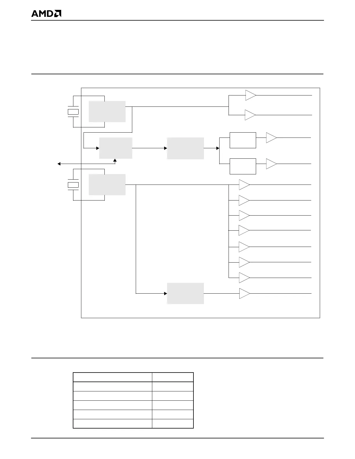
5.2 BLOCK DIAGRAM
Figure 5-1 shows a block diagram of the ÉlanSC520 microcontroller’s internal clocks.
Table 5-1 shows PLL lock times and oscillator start-up times. See the
Élan™SC520
Microcontroller Data Sheet
, order #22003, for timing diagrams and additional clocking
specifications.
Figure 5-1 Clock Source Block Diagram
Table 5-1 Clock Start-up and Lock Times
Clock Source Max
32.768-kHz Oscillator 1 s
33-MHz Oscillator 10 ms
PLL1 (1.47456 MHz) 10 ms
PLL2 (36.864 MHz) 100 µs
PLL3 (66 MHz) 50 µs
32.768-kHz
Crystal
32.768-kHz
Oscillator
PLL2
1.47456 MHz
DIV 31
DIV 2
1.1882-MHz PIT
18.432-MHz UART
33-MHz
Oscillator
PLL3
32.768-kHz SDRAM Refresh
33-MHz
Crystal
36.864 MHz
LF_PLL1
32.768-kHz RTC
Notes:
1. Includes the programmable interval timer (PIT), general-purpose timers, watchdog timer, and the software timer.
PCI
CPU
SDRAM
GP Bus
GP DMA
ROM
SSI
33 MHz
33 MHz
33 MHz
33 MHz
33 MHz
33 MHz
66 MHz
PLL1
Timers
1
33 MHz