General-Purpose Bus Controller
13-4 Élan™SC520 Microcontroller User’s Manual
13.3.1 GP Bus Loading
As more external devices are connected to the GP bus, loading on GPA25
±
GPA0 and
GPD15
±
GPD0 will increase. Therefore, the rise time and fall time of GPA25
±
GPA0 and
GPD15
±
GPD0 will increase, and external buffers may be needed to reduce the loading.
The GP bus provides the GPDBUFOE
pin for external buffer control to reduce the loading.
This signal is asserted for all accesses to external GP bus peripherals. It is not asserted
during accesses to the internal peripherals (regardless of the GP bus echo mode setting).
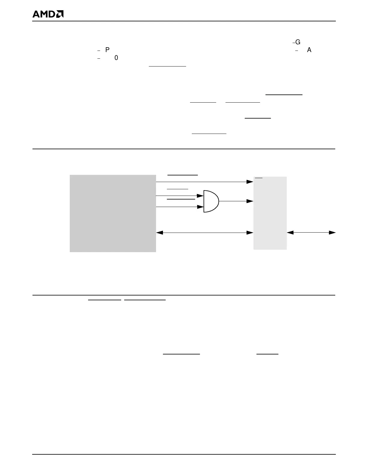
Figure 13-2 shows an example using an external data buffer. The GPDBUFOE
pin can be
used to enable the data buffer, and the GPIORD
or GPMEMRD can be qualified together
to select the direction of the data buffer. If all devices on the GP bus are only I/O-mapped
devices, the AND gate in Figure 13-2 is not required. The GPIORD
pin can be used to
control the direction of the data transceiver. A similar simplification can be applied if all
devices are memory-mapped using the GPMEM
RD pin.
Figure 13-2 Example: Using an External Data Buffer to Address Excess Loading
The GPIOCS16, GPMEMCS16, and GPRDY pins are typically driven by open-drain outputs
from external devices and require a strong pullup resistor (typically 1 Kohm) external to the
ÉlanSC520 microcontroller. The GPIRQx pins also require pullup resistors (typically 1
Kohm).
13.3.2 Voltage Translation
The GP bus provides 5-V- tolerant inputs and 3-V outputs, but if the external devices contain
both 3-V and 5-V devices, the GPDBUFOE
pin qualified with a GPCSx signal can be used
to control the voltage translator. Figure 13-3 shows one example of using a voltage
translator.
GPD15
–
GPD0
GPDBUFOE
Data Bus*
XCVR
DIR
GPIORD
GPMEMRD
EN
Élan™SC520 Microcontroller
Notes:
If the GP address bus must be buffered, ensure that the buffer is always enabled.
* All GP bus peripherals connect their data to this bus.