SDRAM Controller
10-24 Élan™SC520 Microcontroller User’s Manual
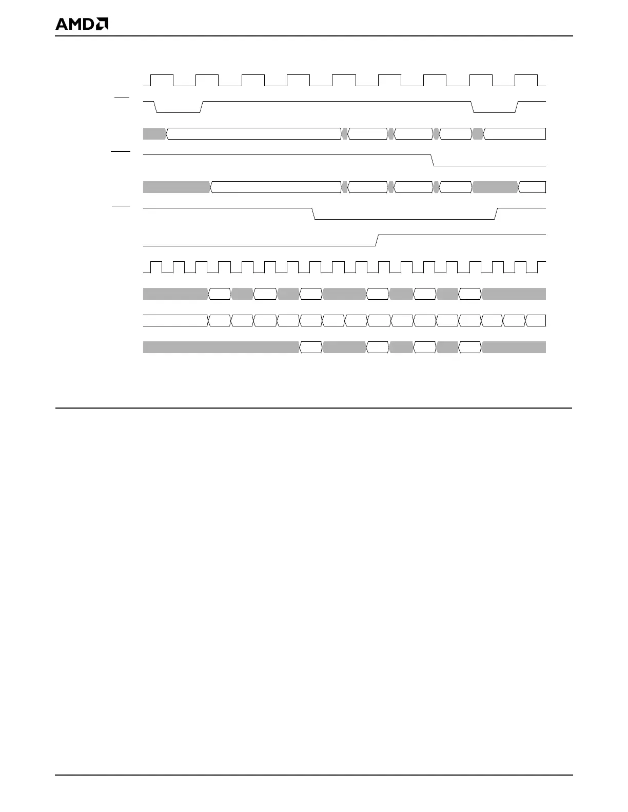
Figure 10-9 SDRAM CPU Burst Write (Write Buffer and ECC Disabled) (Page Miss/Page Hit)
Notes:
This timing diagram does not account for resynchronization of SDRAM signals with CLKMEMIN.
10.5.7.3 ECC SDRAM Cycles
When ECC is enabled, additional overhead is necessary to compensate for ECC logic
delays and read-modify-write cycles due to partial doubleword write cycles. The least
amount of overhead occurs during a full doubleword write to the SDRAM. In the case of a
read, however, the ECC has to generate the new check bits, check for any errors, and
generate an interrupt if an error occurs. A delay of one CPU clock cycle is added for SDRAM
read cycles with ECC enabled. With ECC enabled, read page hit burst timing of 4-1-1-1
(where C
L
= 2) is achieved, compared to a 3-1-1-1 (where C
L
= 2) burst with ECC disabled.
See Figure 10-10 showing the read cycles with ECC enabled.
Wr
04
a
Act
a
Row
b
b
Wr
Col
8
c
Col
c
Wr
Col
C
Pre
Bnk
d
10
1a
Col
Wr
d
clk_cpu
ads
x5_abus
blast
x5_data_out
brdy
pghit
clk_mem
MA12–MA0,
Command
MD31–MD0
BA1–BA0