SDRAM Controller
Élan™SC520 Microcontroller User’s Manual 10-23
10.5.7.2 SDRAM Write Cycle
With the write buffer enabled, all writes to the SDRAM come from the write buffer. With the
write buffer disabled, the SDRAM write cycle could occur due to any of the following reasons:
■ Am5
x
86 CPU
■ ÉlanSC520 microcontroller responding to PCI burst cycle as target
■ GP-DMA
All the writes are configured for single write mode, with each write occurring independently.
Am5
x
86 CPU non-burst write transfers are shown in Figure 10-8. An Am5
x
86 CPU burst
write cycle is shown in Figure 10-9.
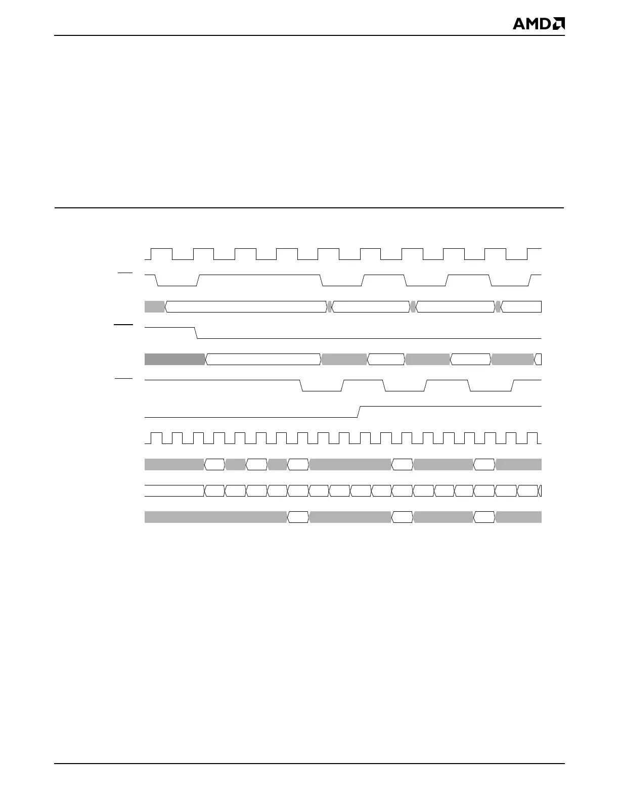
Figure 10-8 SDRAM Write Cycle (Write Buffer and ECC Disabled) (Page Miss/page Hit)
Notes:
This timing diagram does not account for resynchronization of SDRAM signals with CLKMEMIN.
Wr
04
a
Act
a
Row
b
b
Wr
Col
8
c
Col
c
Wr
Col
Pre
Bnk
clk_cpu
ads
x5_abus
blast
x5_data_out
brdy
pghit
clk_mem
MA12–MA0,
Command
MD31–MD0
BA1–BA0