SDRAM Controller
10-12 Élan™SC520 Microcontroller User’s Manual
During read-modify-write cycles, the SDRAM burst read portion of the transaction is
terminated early by the write cycle. This is independent of the enable state of the read-
ahead feature of the read buffer, which is provided to increase read performance by
prefetching data from SDRAM. See “Buffering” on page 10-17 for more information on the
read buffer and associated read-ahead feature.
Write requests to SDRAM always occur as single data transfers, regardless of the amount
of data written by a master. When the write buffer is enabled, all write transactions to SDRAM
are initiated by the write buffer. The write buffer features write merging, write collapsing
and read merging. See “Buffering” on page 10-17 for more information on the write buffer.
10.5.2 SDRAM Addressing
The ÉlanSC520 microcontroller asserts one of the four chip select signals, SCS3–SCS0,
during access to one of the four memory banks. Table 10-7 shows the SDRAM memory
address as a function of the system address for SDRAM devices.
The mapping of the system address into memory row and column addresses is influenced
by the column address configuration provided for each bank.
■ On page misses, a row address followed by a column address is generated during an
SDRAM access.
■ On page hits, only a column address is generated during an SDRAM access.
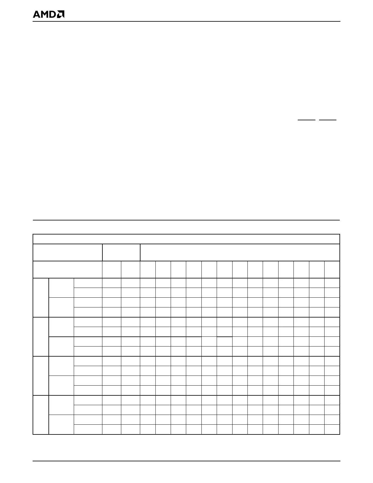
Table 10-7 shows the ÉlanSC520 microcontroller address mapping.
.
Notes: PC refers to SDRAM precharge signaling. BA1–BA0 are the SDRAM Bank Address signals.
Table 10-7 Address Mapping to MAx Signals for SDRAM Devices
SDRAM (16 Mbit–256 Mbit)
SDRAM Configuration
Bank
Selection MAx Pin Mapping
Column Address
Width BA1BA01211109876543210
8 2-bank Row
24 10 23 22 13 12 11 21 20 19 18 17 16 15 14
Column
24 10 PC111098765432
4-bank Row
22 10 24 23 13 12 11 21 20 19 18 17 16 15 14
Column
22 10 PC111098765432
9 2-bank Row 25 11 24 23
13 12 22 21 20 19 18 17 16 15 14
Column
25 11 PC111098765432
4-bank Row 23 11 25 24
13 12 22 21 20 19 18 17 16 15 14
Column
23 11 PC111098765432
10 2-bank Row 26 12 25
24 13 23 22 21 20 19 18 17 16 15 14
Column
26 12 PC111098765432
4-bank Row 24 12 26
25 13 23 22 21 20 19 18 17 16 15 14
Column
24 12 PC111098765432
11 2-bank Row 27
13 26 25 24 23 22 21 20 19 18 17 16 15 14
Column
27 13 12 PC111098765432
4-bank Row 25
13 27 26 24 23 22 21 20 19 18 17 16 15 14
Column
25 13 12 PC111098765432