PCI Bus Host Bridge
9-10 Élan™SC520 Microcontroller User’s Manual
The host bridge PCI bus configuration space contains only PCI bus device configuration
header registers, as defined in the PCI bus specification. ÉlanSC520 microcontroller-
specific host bridge configuration registers are memory-mapped in ÉlanSC520
microcontroller configuration space. See Chapter 4, “System Address Mapping”, for further
details on memory-mapped configuration space.
9.5.2.1 Generating PCI Bus Configuration Cycles
A two-step process is required to generate a PCI bus configuration cycle.
1. First, the Am5
x
86 CPU must perform a 32-bit I/O write to the PCI Configuration Address
(PCICFGADR) register (Port 0CF8h) with the following information: bus number, device
number, function, and register number (doubleword) to be accessed (see Figure 9-7).
2. Then, the Am5
x
86 CPU can perform an I/O cycle (read or write) to the PCI Configuration
Data (PCICFGDATA) register (Port 0CFCh) to access the desired configuration register.
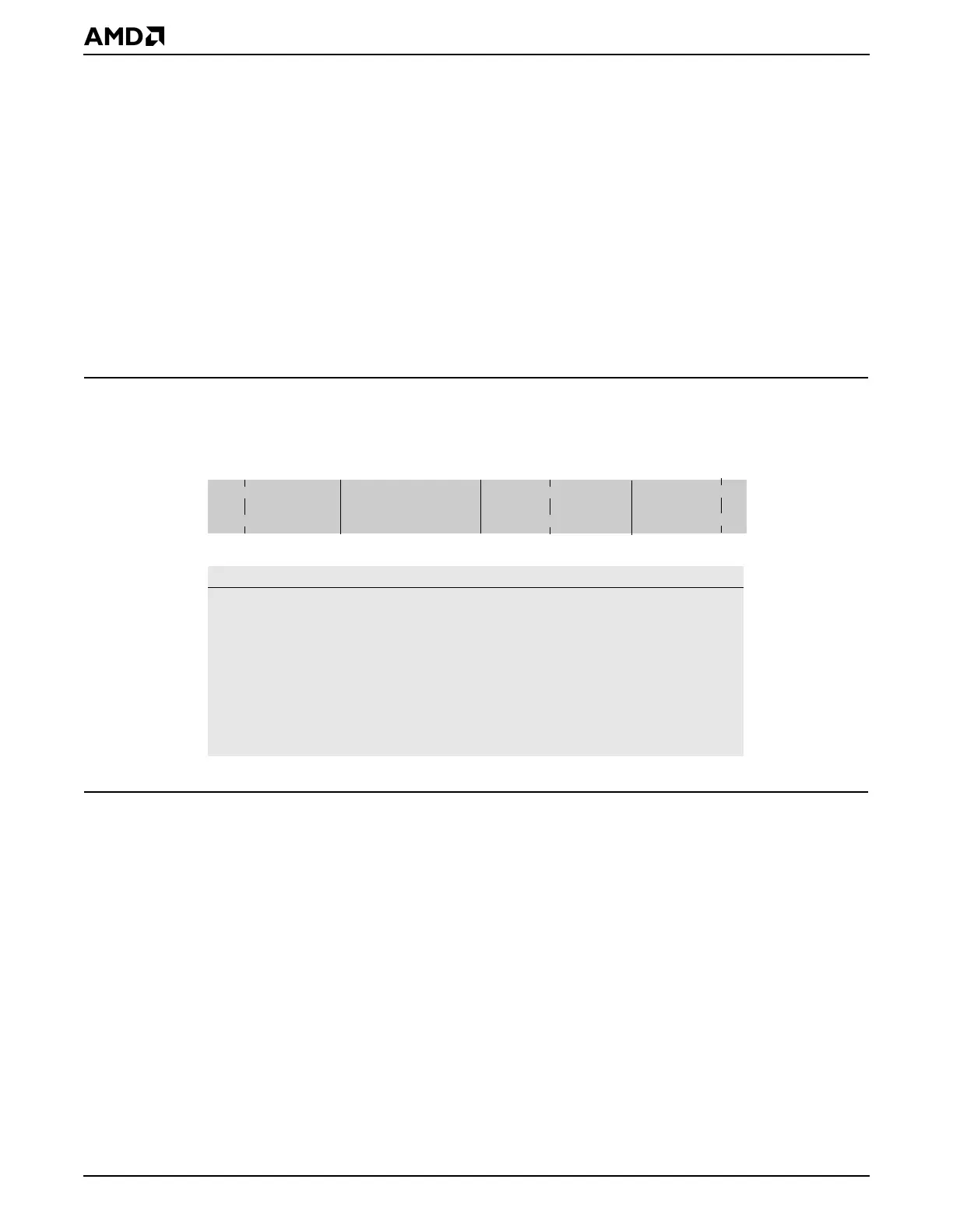
Figure 9-7 PCI Configuration Address (PCICFGADR) Register
For example, to access the Status/Command (PCISTACMD) register (PCI index 04h)
(doubleword 1) of the PCI host bridge, the following cycles are generated by the Am5
x
86
CPU:
1. 32-bit I/O write to Port 0CF8h: 80000004h
– ENABLE = 1 to enable configuration space mapping
– BUS_NUM = 0 (PCI host bridge is on bus number 0)
– DEVICE_NUM = 0 (PCI host bridge is hardwired to device number 0)
– FUNCTION_NUM = 0 (PCI host bridge has only one function)
– REGISTER_NUM = 1
– Bits 1–0 must be written 00
2. 8/16/24/32-bit I/O read/write to/from Port 0CFCh to access configuration register bytes
BUS_NUM[7–0]
REGISTER_
31 15
16
0
Bit Name Function
31 ENABLE This bit must be set to 1 to enable configuration
space mapping.
30–24 Reserved
23–16 BUS_NUM[7–0] Bus number
15–11 DEVICE_NUM[4–0] Device number
10–8 FUNCTION_NUM[2–0] Function number
7–2 REGISTER_NUM[4–0] Register number
1–0 Reserved These bits must always be written to 00.
Reserved
30
23
DEVICE_
NUM[4–0]
NUM[4–0]
12
0 0
EN-
24
11 10
87
FUNCTION_
NUM[2–0]
0CFBh
0CFAh
0CF9h
0CF8h
ABLE