SDRAM Controller
Élan™SC520 Microcontroller User’s Manual 10-7
Figure 10-5 shows a lightly loaded system. Typically, this delay can be implemented as fast
buffers, capacitors, series resistors, etc. or as a short.
Figure 10-5 SDRAM Clock Generation
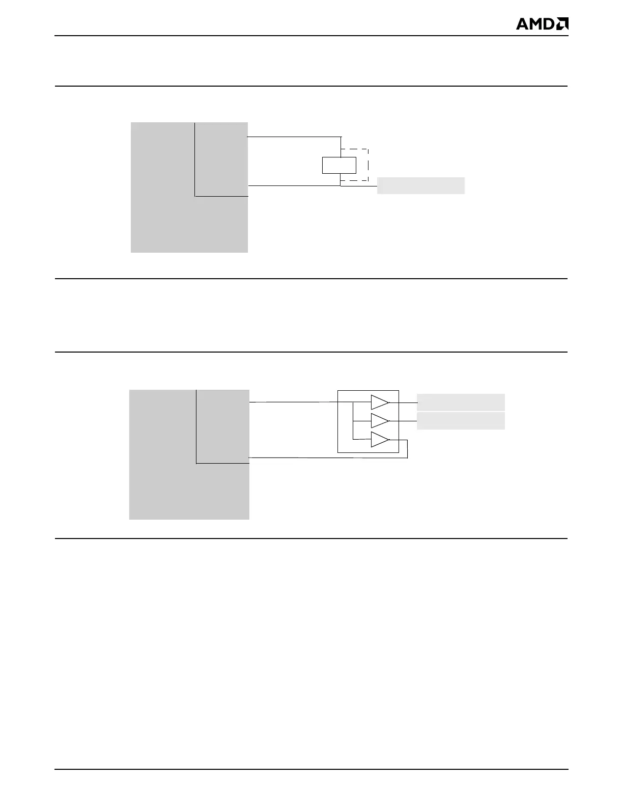
Figure 10-6 shows an example of a two-bank SDRAM system that uses an external clock
driver. The clock driver is used to buffer CLKMEMOUT to support the load of multiple banks
of SDRAM. A buffered version of CLKMEMOUT is returned on CLKMEMIN to compensate
for the clock skew presented by the clock driver.
Figure 10-6 Alternate SDRAM Clock Generation with External Clock Driver
The delays that the system designer must take into consideration are identified by this
equation:
T
AC
+ T
SKEW
+ T
CK_LD
+ T
D_LD
<= T
CK
where:
T
AC
: Access time of SDRAM device (not impacted by board design)
T
SKEW
: The delay between CLKMEMOUT to CLKMEMIN
T
CK_LD
: Additional clock delay due to loading
T
D_LD
: Data delay due to loading
T
CK
: SDRAM memory clock
See the
Élan™SC520 Microcontroller Data Sheet
, order #22003, for timing tables and
additional timing diagrams.
SDRAM
Controller
CLKMEMIN
CLKMEMOUT
Delay
SDRAM Bank
Élan™SC520
Microcontroller
SDRAM Bank
CLKMEMOUT
SDRAM
Controller
CLKMEMIN
Drivers
SDRAM Bank
Élan™SC520
Microcontroller