Write Buffer and Read Buffer
11-2 Élan™SC520 Microcontroller User’s Manual
16-bit contiguous transfers, allowing multiple individual transfers to be merged into a single
transaction to SDRAM.
The read-ahead feature of the read buffer enhances read burst activity by the Am5
x
86 CPU
and external PCI master burst read requests. SDRAM cache line fills by the Am5
x
86 CPU
are probably the most common read requests. These reads typically occur as cache-line
bursts of four doubleword (32-bit) requests. PCI master burst read requests also benefit
greatly.
Each feature can be independently configured. To maintain data coherency, the read buffer
is invalidated during master write cycles or write buffer write cycles that hit an existing line
in the read buffer. Data coherency during all configuration changes of the individual features
is performed in hardware. A manual flush feature of the write buffer is provided.
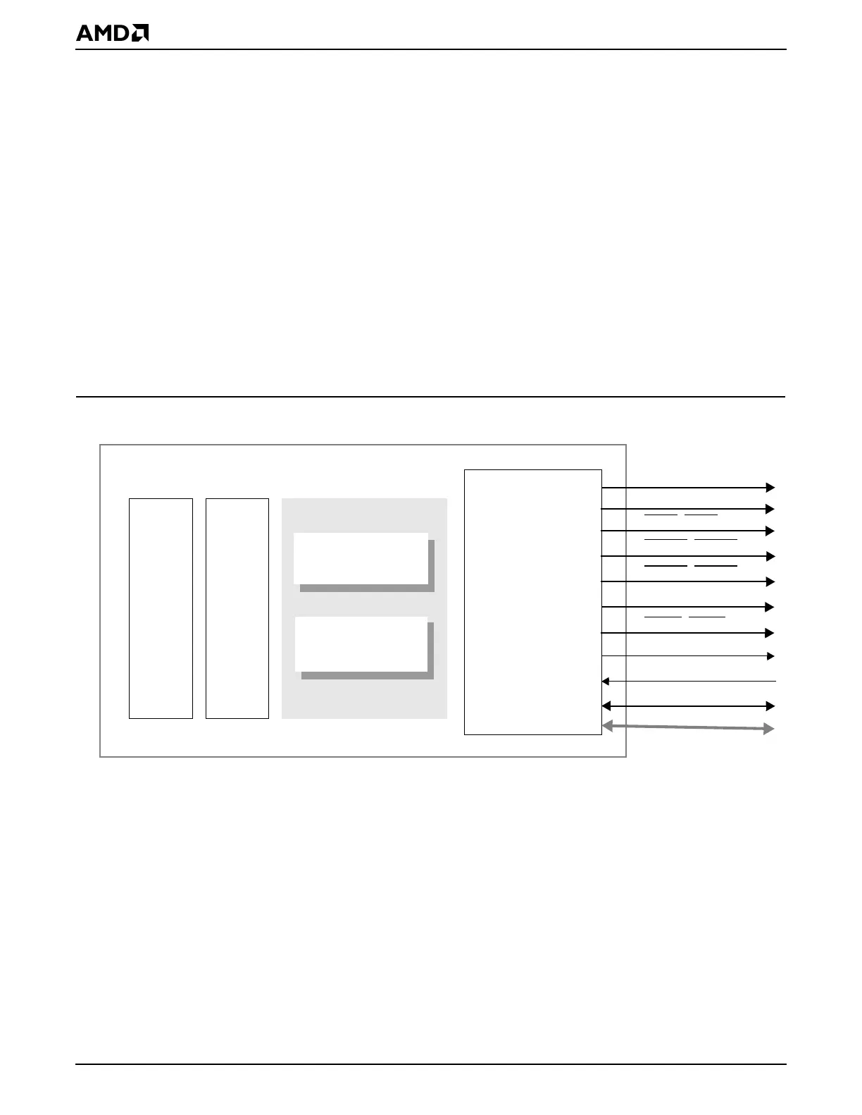
11.2 BLOCK DIAGRAM
The write buffer and read buffer are integrated into the SDRAM controller’s subsystem as
shown in Figure 11-1. Each is capable of functioning independently. A more detailed view
of the internal write buffer and read buffer architecture is shown in Figure 11-2.
Figure 11-1 Write Buffer and Read Buffer Block Diagram (SDRAM Subsystem)
Write Buffer/Read Buffer
SDRAM Controller
Address Decode Unit
CPU Interface
CLKMEMIN
MECC6–MECC0
SDQM3–SDQM0
CLKMEMOUT
MD31–MD0
SCASB–SCASA
SRASB–SRASA
SWEB–SWEA
SCS3–SCS0
MA12–MA0
BA1–BA0
Élan™SC520 Microcontroller
Read Buffer
Write Buffer