System Initialization
3-18 Élan™SC520 Microcontroller User’s Manual
3.7.7 SDRAM Regions
The PAR registers can also be used to define regions of SDRAM and control the read/write,
cacheability, and execution attributes.
3.7.7.1 Setting Up DMA Buffers
Often PCI and GP bus devices use GP-DMA or PCI bus mastering to read and write data
directly from buffers in SDRAM. It is often useful to mark such buffers as noncached. This
can be done using the CPU’s paging unit, but doing so is complex and may conflict with
how an operating system uses the page tables.
In any case, disabling caching for a region is quite simple. Setting the Cacheability Control
Attribute (bit 27) in a PAR register defines a buffer region. For example, a 512-Kbyte region
can be defined to store transmit and receive buffers for a fast Ethernet PCI controller. Since
this is a data-only area, the Code Execution Attribute (bit 28) is set.
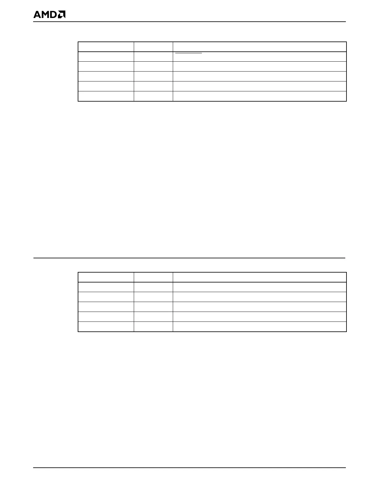
Assuming that the region is located at physical address 00020000h, a PAR register would
be programmed with the value F9FC0020h. This configures the PAR register with the
characteristics shown in Table 3-11.
Of course, this is not absolutely necessary. The cache controller in the ÉlanSC520
microcontroller always maintains the coherency between the cache and SDRAM. For buffer
regions used by GP-DMA channels or PCI bus masters, disabling caching with a PAR
register is more efficient and provides better bus performance than allowing the CPU to
cache the buffer. This avoids the bus activity (and latency) involved with keeping the cache
and the SDRAM coherent.
3.7.7.2 Write-Protected Code Segments
In many embedded systems, all (or most) of the applications and operating system code
is contiguous in memory. In such cases, a single PAR register can be used to write-protect
most (or all) of the code in a system. If errant code attempted to write to the protected
region, then an interrupt would be generated. Note that the CPU completes the write cycle,
but the SDRAM or ROM controller (as appropriate) prevents the write from occurring at the
device.
Table 3-10 Example PAR Programming: Second Bank of Flash for XIP Operating System
Bit Field Value Meaning
Target Device 110b ROMCS2
Attribute Field 000b Write enable, cacheable, code execution allowed
Page Size 1b 64-Kbyte granularity
Region Size 3Fh Specifies sixty-four 64-Kbyte pages for a 4-Mbyte region size
Start Address 80h Physical address 00800000h
Table 3-11 Example PAR Programming: Setting Up DMA Buffers
Bit Field Value Meaning
Target Device 111b SDRAM
Attribute Field 110b Write enable, noncacheable, code execution denied
Page Size 0b 4-Kbyte granularity
Region Size 7Fh Specifies 128 4-Kbyte pages for a 512-Kbyte region size
Start Address 20h Physical address 00200000h