Boundary Scan Test Interface
Élan™SC520 Microcontroller User’s Manual 25-5
25.4.2.2 Bypass Path
This path bypasses the test logic on the microcontroller by reducing the shift length of the
device to one bit. Commands can still be entered in the Instruction register during this
operation.
25.4.2.3 Main Data Scan Path
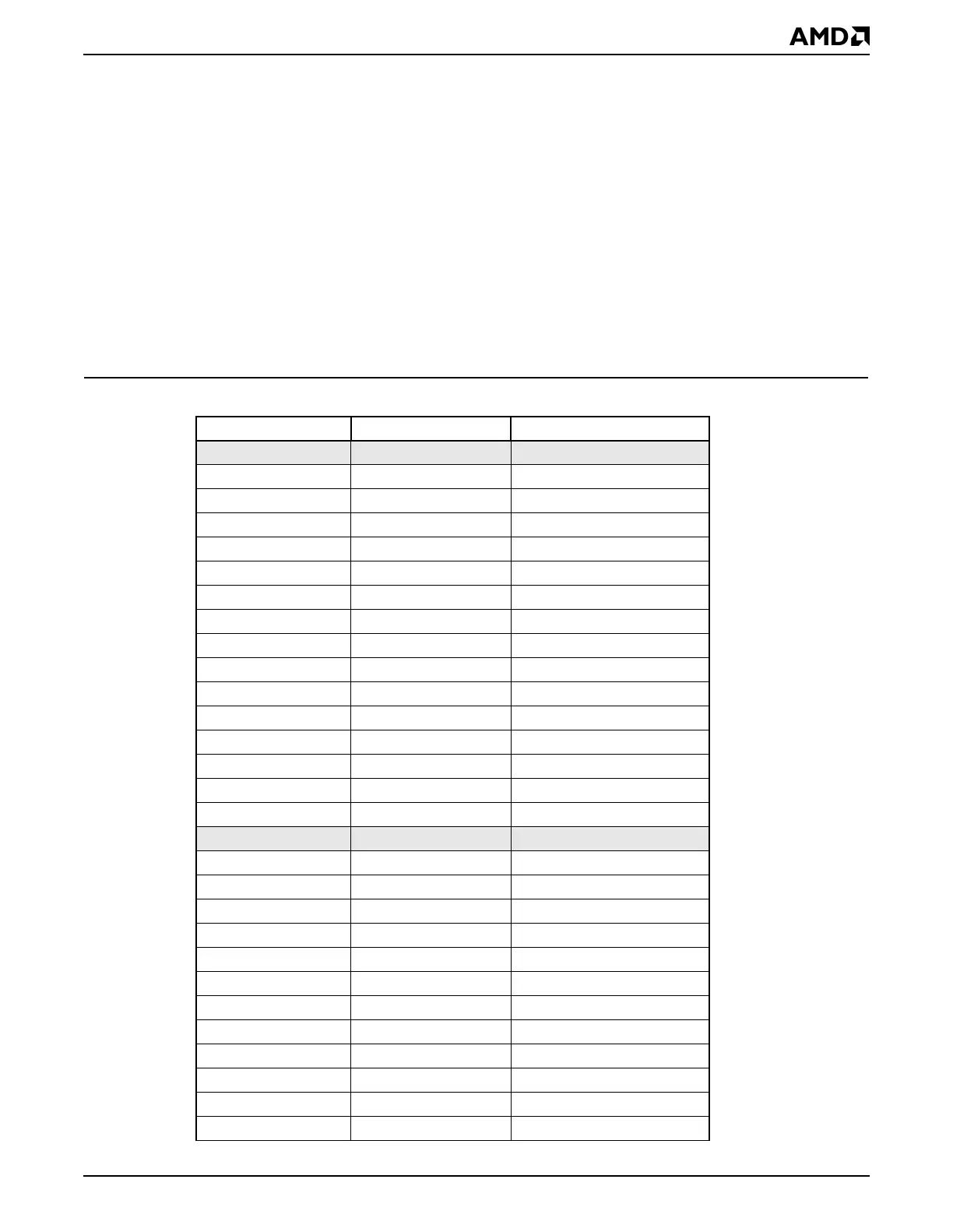
Table 25-3 shows the main data scan path. The order shown is first-to-last; i.e., the first is
closest to JTAG_TDI and the last is closest to JTAG_TDO. Control cells are used to control
the enables of the three-state pads. If a 1 is shifted into the control cell, the associated pins
are three-stated or selected as inputs.
Note: Each of the shaded control cells shown in Table 25-3 contains the output enable
control for the pads listed below the control cell and before the next control cell. For
bidirectional pads, the output is listed first (closest to JTAG_TDI).
Table 25-3 Main Data Scan Path
Pad Name Scan Type Boundary Scan Order
Control 1
BA1 Output 2
BA0 Output 3
MA12 Output 4
MA11 Output 5
MA10 Output 6
MA9 Output 7
MA8 Output 8
MA7 Output 9
MA6 Output 10
MA5 Output 11
MA4 Output 12
MA3 Output 13
MA2 Output 14
MA1 Output 15
MA0 Output 16
Control 17
MD31 Bidirectional 18, 19
MD30 Bidirectional 20, 21
MD29 Bidirectional 22, 23
MD28 Bidirectional 24, 25
MD27 Bidirectional 26, 27
MD26 Bidirectional 28, 29
MD25 Bidirectional 30, 31
MD24 Bidirectional 32, 33
MD23 Bidirectional 34, 35
MD22 Bidirectional 36, 37
MD21 Bidirectional 38, 39
MD20 Bidirectional 40, 41