ROM/Flash Controller
Élan™SC520 Microcontroller User’s Manual 12-3
The ROMCS1 and ROMCS2 signals are provided to support two additional ROM chip
selects. These pins are shared with general-purpose chip selects, GPCS1
and GPCS2,
respectively, as shown in Table 12-2. When enabled, the multiplexed signals shown in
Table 12-2 either disable or alter any other function that uses the same pin.
The ROM controller can accommodate various performance and system voltage isolation
requirements. Depending on the operation voltage required by the ROM and the voltage
required by other devices sharing the same bus, the ROM data pins can be connected
either to the GP bus or to the SDRAM interface (see Figure 12-2). Note that the ROM data
pins must connect to only one interface per chip select (i.e., the ROM data pins may not
straddle the two buses).
■ Devices can be placed on the SDRAM bus to gain the advantage of a 32-bit data path.
However, care must be taken by the system designer because of SDRAM loading and
timing issues. See “System Design” on page 10-1.
■ Alternately, the ROM devices can be implemented on the GP bus data pins. These
devices are limited to 8- or 16-bits. See Table 12-1 for data width connection options.
Note that the addresses for ROM devices are always provided via GP bus, independently
of whether the data pins of the ROM are connected to the GP bus or SDRAM bus.
12.3.1 Voltage Isolation
From the ÉlanSC520 microcontroller’s perspective, both the SDRAM bus and the GP bus
are 5-V-tolerant and drive 3.3 V. However, an isolation buffer is necessary when using the
same bus for 5-V ROM devices and 3.3-V SDRAM devices that are not 5-V-tolerant. For
example, if the 3.3-V SDRAM devices are not 5-V-tolerant and share the data bus with
5-V ROM devices, the 3.3-V SDRAM devices could be damaged during ROM read access
if an isolation buffer is not used.
The ROMBUFOE
signal is provided to support an isolation buffer, and this signal can be
used for devices on the SDRAM bus or the GP bus. Some scenarios for such a situation
are shown in Figure 12-2. The ROMBUFOE
signal asserts during all accesses to ROM
devices, whether the devices are located on the SDRAM bus or the GP bus.
Note that the SDRAM controller’s read and write buffers are not utilized during accesses
to ROM devices. This is true even if a ROM device is located on the SDRAM bus. When
the SDRAM buffering is enabled, the ROM devices connected to the SDRAM data bus
(MD31– MD0), must use ROMRD
to control the ROM device’s data pins. In this case, the
system design should ensure that the external device does not drive data while ROMRD
is deasserted.
When sharing the SDRAM data bus with ROM devices, the loading of the data bus requires
careful consideration. A buffer should be used on the data bus to prevent heavy loading
by the ROM devices. In a system that utilizes buffering of these devices, the ROMBUFOE
signal can be used to control the buffers. Similarly, data buffers can be used on the GP bus
to control loading issues, and the ROMBUFOE
pin should still be used to control buffers in
front of these ROM devices.
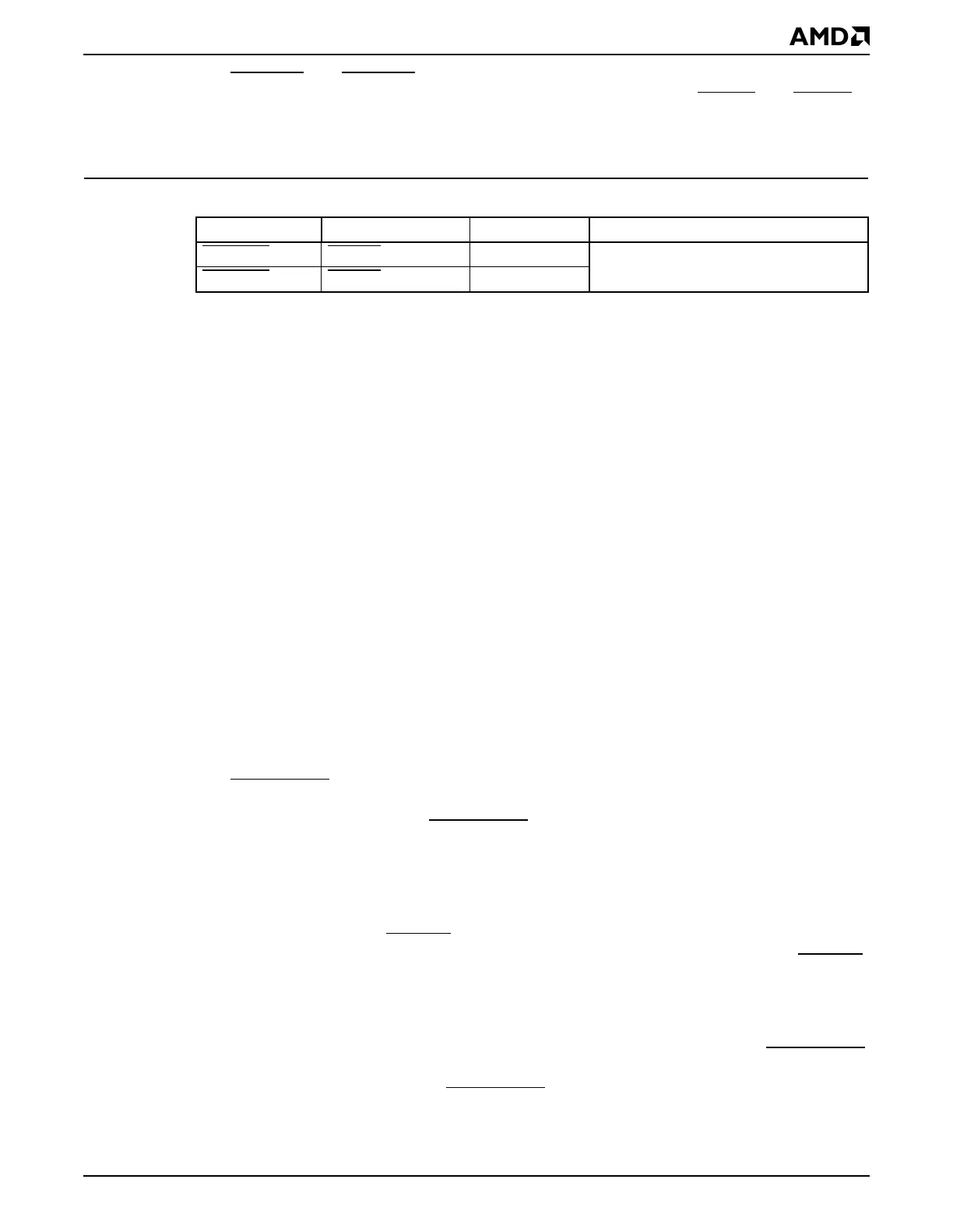
Table 12-2 ROM Signals Shared with Other Interfaces
Default Signal Alternate Function Control Bit Register
ROMCS2
GPCS2 GPCS2_SEL Chip Select Pin Function Select
(CSPFS) register (MMCR offset C24h)
ROMCS1
GPCS1 GPCS1_SEL