System Address Mapping
4-2 Élan™SC520 Microcontroller User’s Manual
■ Integrated PC/AT compatible peripherals are direct-mapped in normal PC I/O space
(i.e., the programmable interrupt controller, programmable interval timer, GP bus DMA
controller, RTC, and UARTs). All remaining integrated peripherals are memory-mapped
(the watchdog timer, software timer, GP timers, and SSI).
■ As a PCI target, the PCI bus host bridge decodes normal SDRAM address space,
allowing external PCI bus master access of the entire SDRAM space. PCI bus I/O
accesses from PCI masters are not decoded by the PCI host bridge.
4.2 REGISTERS
Address decoding is controlled by the configuration registers listed in Table 4-1 and
Table 4-2.
I
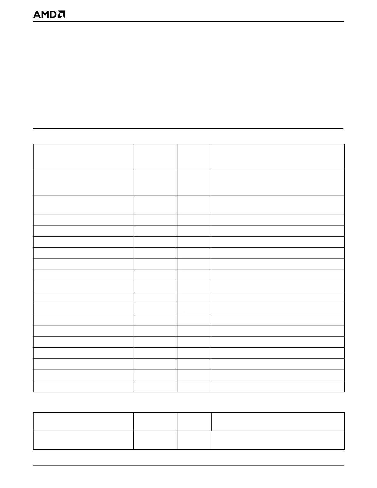
Table 4-1 Address Decoding Registers—Memory-Mapped
Register Mnemonic
MMCR
Offset
Address Function
Address Decode Control ADDDECCTL 80h RTC disable, UART 1 and UART 2 disables,
write protect violation interrupt enable, I/O hole
access destination
Write-Protect Violation Status WPVSTA 82h Write-protect violation interrupt status, master,
window number
Programmable Address Region 0 PAR0 88h General-purpose resource decoding
Programmable Address Region 1 PAR1 8Ch General-purpose resource decoding
Programmable Address Region 2 PAR2 90h General-purpose resource decoding
Programmable Address Region 3 PAR3 94h General-purpose resource decoding
Programmable Address Region 4 PAR4 98h General-purpose resource decoding
Programmable Address Region 5 PAR5 9Ch General-purpose resource decoding
Programmable Address Region 6 PAR6 A0h General-purpose resource decoding
Programmable Address Region 7 PAR7 A4h General-purpose resource decoding
Programmable Address Region 8 PAR8 A8h General-purpose resource decoding
Programmable Address Region 9 PAR9 ACh General-purpose resource decoding
Programmable Address Region 10 PAR10 B0h General-purpose resource decoding
Programmable Address Region 11 PAR11 B4h General-purpose resource decoding
Programmable Address Region 12 PAR12 B8h General-purpose resource decoding
Programmable Address Region 13 PAR13 BCh General-purpose resource decoding
Programmable Address Region 14 PAR14 C0h General-purpose resource decoding
Programmable Address Region 15 PAR15 C4h General-purpose resource decoding
Table 4-2 Address Decoding Registers—Direct-Mapped
Register Mnemonic
I/O
Address Function
Configuration Base Address CBAR FFFCh Base address for the alias of the MMCR
registers