GP Bus DMA Controller
14-4 Élan™SC520 Microcontroller User’s Manual
14.4 REGISTERS
The GP bus DMA (GP-DMA) controller is configured using memory-mapped registers and
direct-mapped registers.
14.4.1 Memory-Mapped Registers
A summary listing of the MMCR registers used to configure the GP-DMA controller is shown
in Table 14-2. These registers provide functionality beyond the PC/AT compatibility, such
as the extended page registers, the features in the enhanced GP-DMA mode, and the
ability to route external GPDRQx and GPDACKx
signals to a specific channel of the GP-
DMA controller.
Table 14-1 GP-DMA Signals Shared with Other Interfaces
PIO
(Default)
Signal
Interface
Function Control Bit Register
PIO12 GPDACK0
PIO12_FNC PIO15–PIO0 Pin Function Select
(PIOPFS15_0) register (MMCR offset C20h)
PIO11 GPDACK1
PIO11_FNC
PIO10 GPDACK2
PIO10_FNC
PIO9 GPDACK3
PIO9_FNC
PIO8 GPDRQ0 PIO8_FNC
PIO7 GPDRQ1 PIO7_FNC
PIO6 GPDRQ2 PIO6_FNC
PIO5 GPDRQ3 PIO5_FNC
PIO4 GPTC PIO4_FNC
PIO3 GPAEN PIO3_FNC
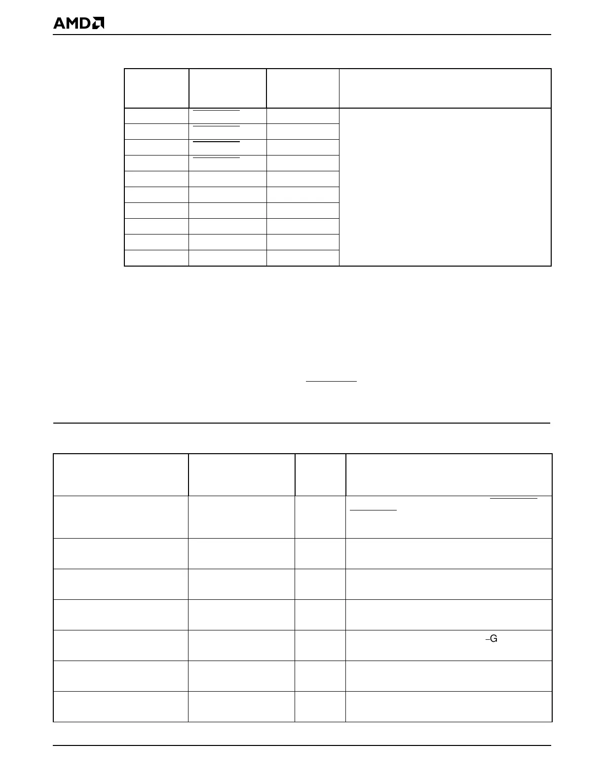
Table 14-2 GP-DMA Controller Registers—Memory-Mapped
Register Mnemonic
MMCR
Offset
Address Function
PIO15–PIO0 Pin Function
Select
PIOPFS15_0 C20h PIO or interface function select: GPDACK3
–
GPDACK0
, GPDRQ3–GPDRQ3, GPTC,
GPAEN
DMA Buffer Chaining
Interrupt Mapping
DMABCINTMAP D40h GP-DMA buffer chaining interrupt mapping
GP-DMA Control GPDMACTL D80h GP-DMA enhanced mode enable, channel
size, clock mode
GP-DMA Memory-Mapped
I/O
GPDMAMMIO D81h I/O or memory-mapped I/O channel
configuration
GP-DMA Resource Channel
Map A
GPDMAEXTCHMAPA D82h Channel mapping for GPDRQ3
±
GPDRQ0
GP-DMA Resource Channel
Map B
GPDMAEXTCHMAPB D84h Channel mapping for internal serial port
GP-DMA requests
GP-DMA Channel 0
Extended Page
GPDMAEXTPG0 D86h Bits 27–24 of the memory address for
Channel 0