PCI Bus Host Bridge
Élan™SC520 Microcontroller User’s Manual 9-17
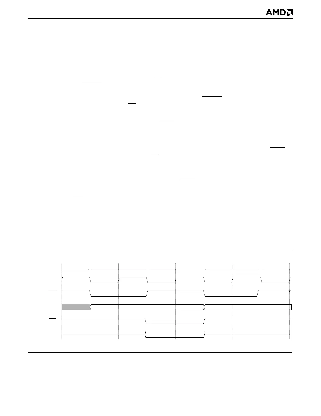
The following sequence annotates the Am5
x
86 CPU non-posted write cycle to the PCI bus
shown in Figure 9-11.
■ Clock #1: The Am5
x
86 CPU starts a write cycle to the PCI bus.
■ Clock #6: The PCI host bridge master controller has synchronized the Am5
x
86 CPU
bus request and asserts req
to gain access to the PCI bus. Because the Am5
x
86 CPU
is the initiator of the cycle, the bus request signal is not seen externally.
■ Clock #7: The PCI host bridge gnt signal is sampled asserted, and the PCI bus is idle,
so FRAME
is asserted to begin the PCI bus transaction. In this example, there is no
arbitration delay (the arbiter is parked on the host bridge). If another external PCI bus
master was granted the bus, or the bus was not idle FRAME
assertion would be delayed
until the host bridge’s gnt
was asserted and the bus was idle. Because the Am5
x
86 CPU
is the initiator of the cycle, the bus request signal is not seen externally.
■ Clock #9: The PCI target asserts TRDY, indicating it can accept the write data. In this
example, the PCI bus target did not add any wait states to the transaction. A PCI bus
Revision 2.2 compliant target can add up to 16 wait states that would delay the
transaction completion. A PCI bus target can also retry the transaction. In this case, the
host bridge continues to generate the same transaction until the target returns TRDY
to
complete the transaction. The rdy
signal is not returned to the Am5
x
86 CPU until the
PCI bus transaction completes. See Section 9.5.3.4.2 for information on retried
transactions.
■ Clock #10: The PCI host bridge samples TRDY asserted, which ends the transaction.
■ Clock #12: The Am5
x
86 CPU bus synchronizes the end of the PCI bus cycle and asserts
rdy
to the Am5
x
86 CPU, which ends the write cycle.
9.5.3.4.5 PCI Bus Configuration Read/Write
Am5
x
86 CPU write cycles to the PCI Configuration Address (PCICFGADR) register (Port
0CF8h) or the PCI Configuration Data (PCICFGDATA) register (Port 0CFCh) for internal
PCI host bridge configuration complete with zero Am5
x
86 CPU cycle wait states (see
Figure 9-12).
Figure 9-12 CPU Write Cycles to Internal PCI Bus Configuration Registers
Am5
x
86 CPU read cycles from the PCI Configuration Address (PCICFGADR) register or
PCI Configuration Data (PCICFGDATA) register for internal PCI host bridge configuration
registers also complete with zero wait states (see Figure 9-13). See the read and write
timing diagrams in Figure 9-8 through Figure 9-11 for Am5
x
86 CPU read and writes cycles
1 2 3 4
cfg write data
clk_cpu
ads
cycle_info
rdy
Data