SDRAM Controller
10-18 Élan™SC520 Microcontroller User’s Manual
demanded access to be read into the read buffer. GP-DMA read accesses are
always
single
word accesses.
The read buffer is always enabled, however, the read-ahead feature and write buffer can
be independently enabled and are disabled after a system reset or programmable reset.
For more information on the SDRAM controller’s buffering, see Chapter 11, “Write Buffer
and Read Buffer”.
10.5.5 SDRAM Control Configuration
The SDRAM controller provides the following control functions:
■ Refresh rate
■ Refresh enable
■ SDRAM pin drive strength
■ Write buffer test mode
■ Operation mode select
10.5.5.1 Refresh Control
To refresh the SDRAM devices, the SDRAM controller issues the Auto Refresh command.
Since the ÉlanSC520 microcontroller is intended to support a variety of vendors, the refresh
rate at which this command is issued is a configurable parameter. It is specified in the
DRAM Refresh Request Speed (RFSH_SPD) bit field in the SDRAM Control (DRCCTL)
register (MMCR offset 10h) and offers either 7.8-µs, 15.6-µs, 31.2-µs or 62.5-µs periods.
Note: Since the minimum refresh rate is 62.5
µ
s, which is below the maximum time between
an Active command and a Precharge command (T
RAS
), the SDRAM controller does not
support a RAS
time-out feature.
The refresh rate is calculated from this equation:
Refresh Rate = Interval / Row
where:
Interval is how often a particular row must be refreshed
Row is the number of rows within the device that must be refreshed
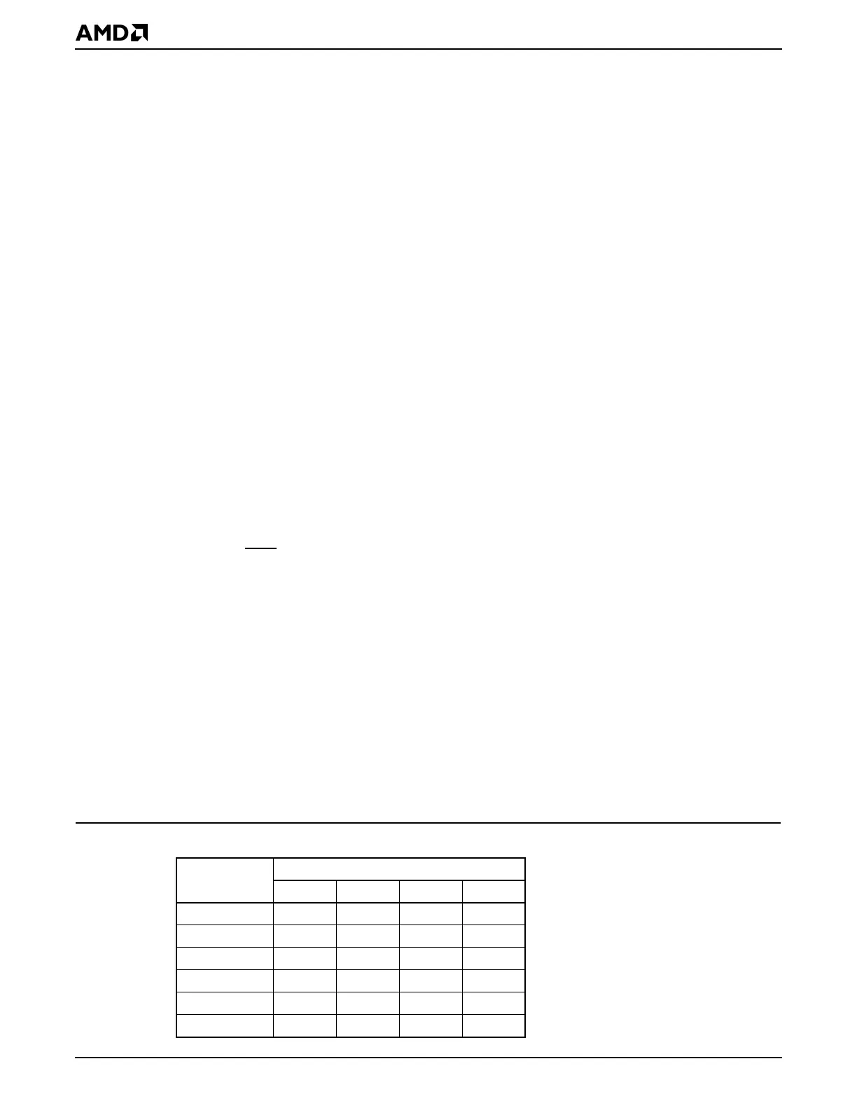
Table 10-11 shows the SDRAM refresh rates and their corresponding intervals. SDRAM
devices contain either two or four internal banks. During each refresh cycle, all internal
SDRAM banks are refreshed simultaneously. This implies that a 2-bank architecture
performs dual-row refresh and a 4-bank architecture performs a quad-row refresh, per
refresh cycle.
Table 10-11 SDRAM Refresh Rates
Number of
Rows
Refresh Rate
7.8 µs 15.6 µs 31.2 µs 62.5 µs
256 2 ms 4 ms 8 ms 16 ms
512 4 ms 8 ms 16 ms 32 ms
1024 8 ms 16 ms 32 ms 64 ms
2048 16 ms 32 ms 64 ms 128 ms
4096 32 ms 64 ms 128 ms
8192 64 ms 128 ms