General-Purpose Timers
Élan™SC520 Microcontroller User’s Manual 17-5
17.5.4 Configuration Information
The GP Timer x Count (GPTMRxCNT) registers contain the current value of a timer. These
registers can be read or written at any time, regardless of whether the corresponding timer
is running. The timer increments the value of the corresponding GP Timer x Count
(GPTMRxCNT) register each time a timer event occurs.
Each timer has a GP Timer x Maxcount Compare A (GPTMRxMAXCMPA) register that
defines the maximum value of the timer.
■ When the timer reaches the maximum value, it resets the GP Timer x Count
(GPTMRxCNT) register value to 0 during the same clock cycle.
■ The value in the GP Timer x Count (GPTMRxCNT) register never equals the GP Timer
x Maxcount Compare A (GPTMRxMAXCMPA) register.
In addition, timers 0 and 1 have a secondary GP Timer x Maxcount Compare B
(GPTMRxMAXCMPB) register.
■ Using both the primary GP Timer x Maxcount Compare A (GPTMRxMAXCMPA) register
and the secondary GP Timer x Maxcount Compare B (GPTMRxMAXCMPB) register
lets the timer alternate between two maximum values. This is called
alternate compare
mode
. It is controlled by the ALT_CMP bit in the GP Timer x Mode/Control (GPTMRxCTL)
register.
– If the timer is programmed to use both of its GP Timer Maxcount Compare registers,
and the ALT_CMP and CONT_CMP bits are set in the GP Timer x Mode/Control
(GPTMRxCTL) register, the timer output pin (TMROUT0 or TMROUT1) generates a
square waveform.
– The duty cycle and frequency of the waveform depend on the values in the alternating
GP Timer Maxcount Compare registers.
■ If the timer is programmed with the ALT_CMP bit to use only the primary GP Timer x
Maxcount Compare A (GPTMRxMAXCMPA) register, the timer output pin (TMROUT0
or TMROUT1) switches Low for a single Am5
x
86 CPU clock cycle after the maximum
value is reached.
17.5.5 Clocking Considerations
The clock source for the three general-purpose timers is the 33-MHz system clock. For GP
Timer 0 and GP Timer 1, the clock source can also be an external pin or a derived prescale
clock. This option is specified in the GP Timer 0 Mode/Control (GPTMR0CTL) register
(MMCR offset C72h) and the GP Timer 1 Mode/Control (GPTMR1CTL) register (MMCR
offset C7Ah).
17.5.5.1 Internal Clock
The resolution range of the internal clock depends on which 33-MHz crystal is used in the
system, as shown in Table 17-3.
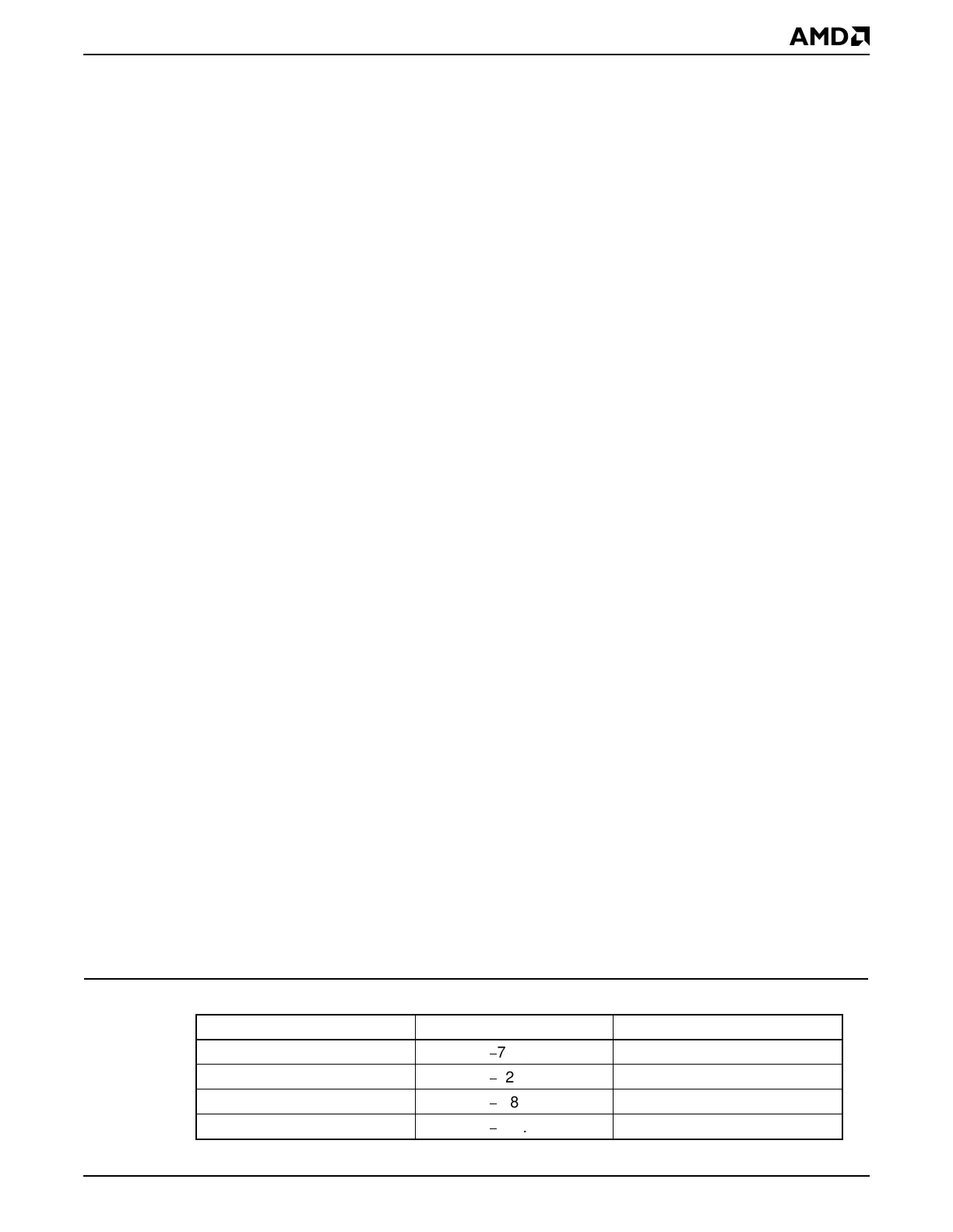
Table 17-3 GP Timers Internal Clock Sources
Internal Clock Source Resolution Range Duration
33.000 MHz 121.20 ns
±
7.94 ms 16-bit duration
33.000 MHz 121.20 ns
±
520.55 seconds 32-bit duration
33.333 MHz 120.00 ns
±
7.86 ms 16-bit duration
33.333 MHz 120.00 ns
±
515.40 seconds 32-bit duration