Pin Information
Élan™SC520 Microcontroller User’s Manual 2-5
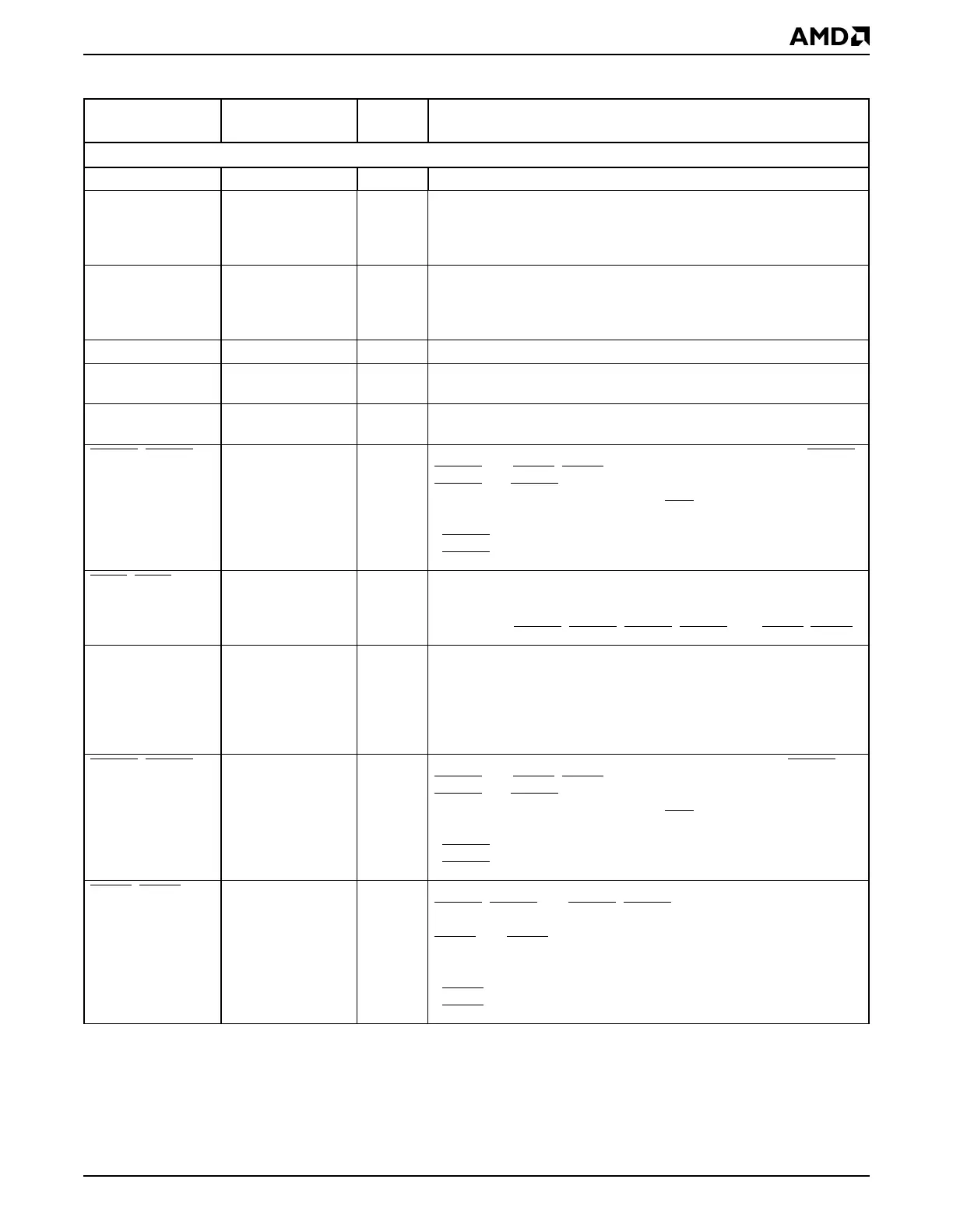
Table 2-2 Signal Descriptions
Signal
Multiplexed
Signal Type Description
Synchronous DRAM Controller
BA1–BA0 — O Bank Address is the SDRAM bank address bus.
CLKMEMIN — I SDRAM Clock Input is the SDRAM clock return signal used to
minimize skew between the internal SDRAM clock and the
CLKMEMOUT signal provided to the SDRAM devices. This signal
compensates for buffer and load delays introduced by the board design.
CLKMEMOUT — O SDRAM Clock Output is the 66-MHz clock that provides clock
signalling for the synchronous DRAM devices. This clock may require
an external Low skew buffer for system implementations that result in
heavy loading on the SDRAM clock signal.
MA12–MA0 — O SDRAM Address is the SDRAM multiplexed address bus.
MD31–MD0 — B SDRAM Data Bus inputs data during SDRAM read cycles and outputs
data during SDRAM write cycles.
MECC6–MECC0 — B Memory Error Correction Code contains the ECC checksum
(syndrome) bits used to validate and correct data errors.
SCASA
–SCASB —OColumn Address Strobes are used in combination with the SRASA–
SRASB
and SWEA–SWEB to encode the SDRAM command type.
SCASA
and SCASB are the same signal provided on two different pins
to reduce the total load connected to CAS
.
Suggested system connection:
SCASA
for SDRAM banks 0 and 1
SCASB
for SDRAM banks 2 and 3
SCS3
–SCS0 —OSDRAM Chip Selects are the SDRAM chip-select outputs. These
signals are asserted to select a bank of SDRAM devices. The chip-
select signals enable the SDRAM devices to decode the commands
asserted via SRASA
–SRASB, SCASA–SCASB, and SWEA–SWEB.
SDQM3–SDQM0 — O Data Input/Output Masks make SDRAM data output high-impedance
and blocks data input on SDRAM while active. Each of the four
SDQM3–SDQM0 signals is associated with one byte of four
throughout the array. Each SDQMx signal provides an input mask
signal for write accesses and an output enable signal for read
accesses.
SRASA
–SRASB —ORow Address Strobes are used in combination with the SCASA–
SCASB
and SWEA–SWEB to encode the SDRAM command type.
SRASA
and SRASB are the same signal provided on two different pins
to reduce the total load connected to RAS
.
Suggested system connection:
SRASA for SDRAM banks 0 and 1
SRASB
for SDRAM banks 2 and 3
SWEA
–SWEB —OSDRAM Memory Write Enables are used in combination with the
SRASA
–SRASB and SCASA–SCASB to encode the SDRAM
command type.
SWEA
and SWEB are the same signal provided on two different pins
to reduce the total load connected to WE.
Suggested system connection:
SWEA
for SDRAM banks 0 and 1
SWEB
for SDRAM banks 2 and 3