SDRAM Controller
Élan™SC520 Microcontroller User’s Manual 10-25
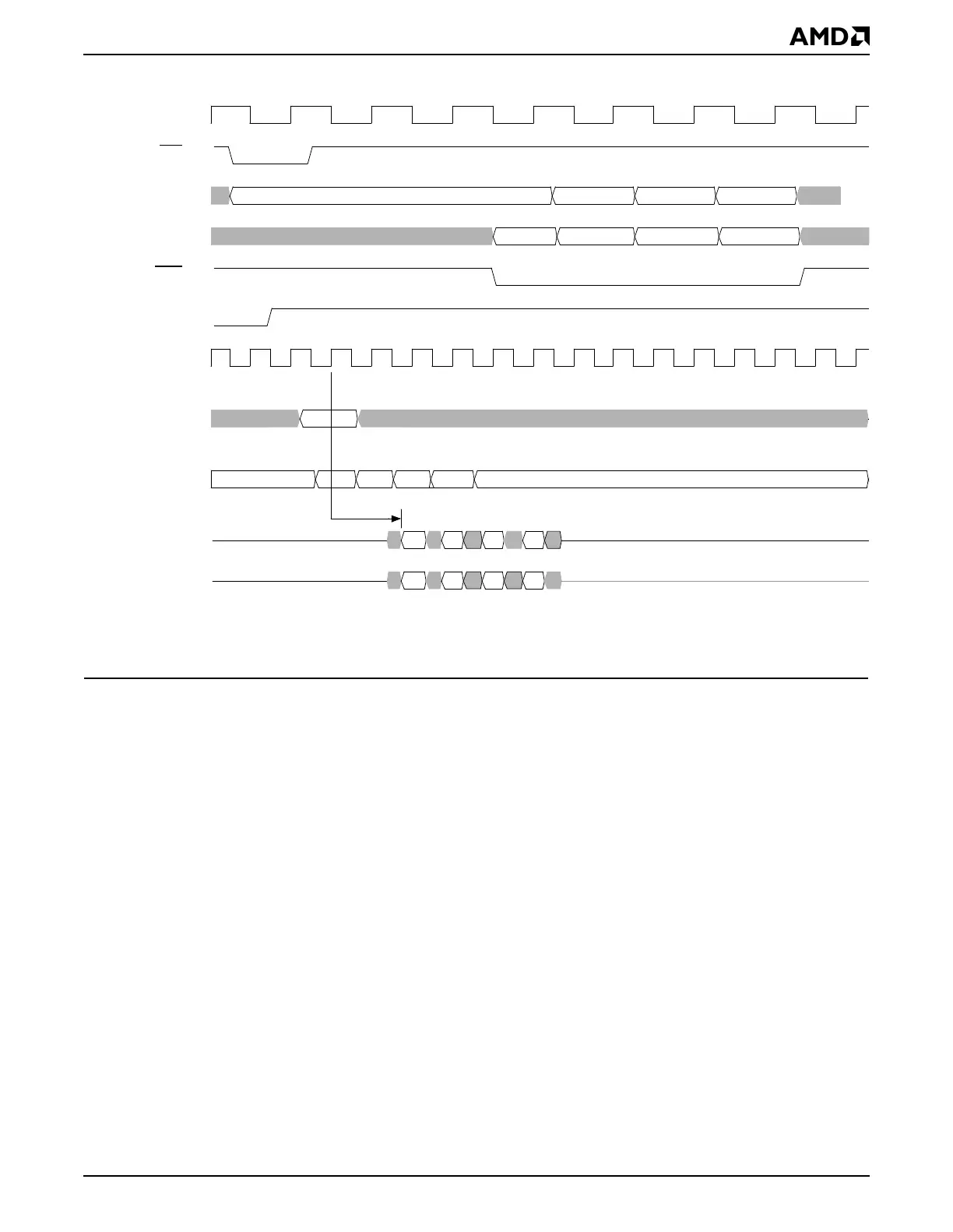
Figure 10-10 SDRAM Burst Read Cycle with ECC Enabled
Notes:
This timing diagram does not account for resynchronization of SDRAM signals with CLKMEMIN.
The ECC overhead is even higher in the case of a read-modify-write cycle, as shown in
Figure 10-11. As shown, a write cycle with a partial doubleword requires an SDRAM read
cycle followed by a write cycle. Note that the SDRAM read burst is terminated early by the
write cycle. See “Error Correction Code (ECC)” on page 10-16 for details of a read-modify-
write cycle.
CAS latency = 2
4
8
C
a
bc d
0
ab
c
d
clk_cpu
ads
x5_abus
x5_data_in
brdy
pghit
clk_mem
MA12–MA0,
Command
MD31–MD0
MECC6–
Rd
BA1–BA0
MECC0
Col