General-Purpose Bus Controller
Élan™SC520 Microcontroller User’s Manual 13-5
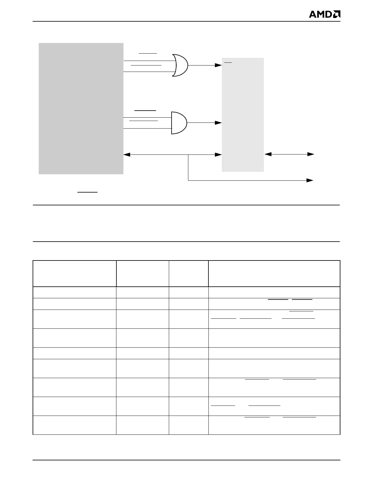
Figure 13-3 Example: Using a Voltage Translator
13.4 REGISTERS
Table 13-2 shows the memory-mapped registers used to configure the GP bus controller.
Table 13-2 GP Bus Registers—Memory-Mapped
Register Mnemonic
MMCR
Offset
Address Function
GP Echo Mode GPECHO C00h Echo mode enable
GP Chip Select Data Width GPCSDW C01h Data width select for GPCS7
–GPCS0
GP Chip Select Qualification GPCSQUAL C02h Chip select qualification with GPIORD,
GPIOWR
, GPMEMRD, or GPMEMWR
GP Chip Select Recovery
Time
GPCSRT C08h Chip select recovery time of a GP bus cycle
GP Chip Select Pulse Width GPCSPW C09h Width of the chip select signal from the offset
GP Chip Select Offset GPCSOFF C0Ah Chip select offset time from the beginning of the
bus cycle
GP Read Pulse Width GPRDW C0Bh Width of the GPIORD
and GPMEMRD signals
from the offset
GP Read Offset GPRDOFF C0Ch Offset from the beginning of the bus cycle for
GPIORD
and GPMEMRD
GP Write Pulse Width GPWRW C0Dh Width of the GPIOWR and GPMEMWR signals
from the offset
GPD15
–
GPD0
GPDBUFOE
5-V Data
Voltage
DIR
GPIORD
GPMEMRD
EN
GPCSx
Translator
3-V Data
XCVR
Élan™SC520 Microcontroller
Notes:
GPCSx
is the chip select for the 5-V peripheral.