SDRAM Controller
10-10 Élan™SC520 Microcontroller User’s Manual
10.4 REGISTERS
A summary listing of the registers used to control the SDRAM configuration are shown in
Table 10-6.
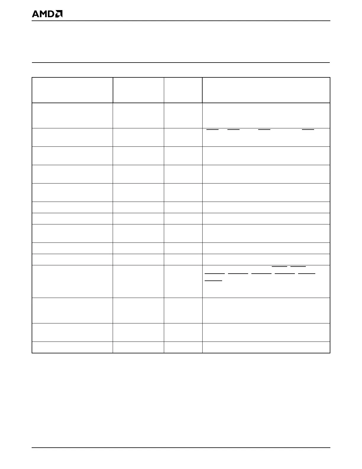
Table 10-6 SDRAM Controller Registers—Memory-Mapped
Register Mnemonic
MMCR
Offset
Address Function
SDRAM Control DRCCTL 10h Operation mode select, refresh enable, refresh
rate select, SDRAM write buffer test mode
enable
SDRAM Timing Control DRCTMCTL 12h RAS
-to-CAS delay, RAS precharge, CAS
latency
SDRAM Bank Configuration DRCCFG 14h Bank count select, address column width
requirements for each bank
SDRAM Bank 0–3 Ending
Address
DRCBENDADR 18h Independent bank ending configurations and
enables for banks 0, 1, 2 and 3
ECC Control ECCCTL 20h ECC enable, interrupt enable for single-bit and
multi-bit error detection
ECC Status ECCSTA 21h Single-bit and multi-bit error status
ECC Check Bit Position ECCCKBPOS 22h ECC data bit position in check bit or data bit fields
ECC Check Code Test ECCCKTEST 23h ECC check code override for test and error
handler development
ECC Single-Bit Error Address ECCSBADD 24h Address where single-bit ECC error occurred
ECC Multi-Bit Error Address ECCMBADD 28h Address where multi-bit ECC error occurred
Drive Strength Control DSCTL C28h I/O pad drive strength for SCS3
–SCS0,
SRASA
–SRASB, SCASA–SCASB, SWEA–
SWEB
, SDQM3–SDQM0, MA12–MA0, BA1–
BA0, MD31–MD0, MECC6–MECC0
ECC Interrupt Mapping ECCMAP D18h ECC interrupt mapping to any of 22 available
interrupt channels or NMI, ECC NMI enable
control
Reset Configuration RESCFG D72h Programmable SDRAM retention reset
(PRGRESET pin enable)
Reset Status RESSTA D74h Reset source status: PRGRESET pin