System Initialization
3-10 Élan™SC520 Microcontroller User’s Manual
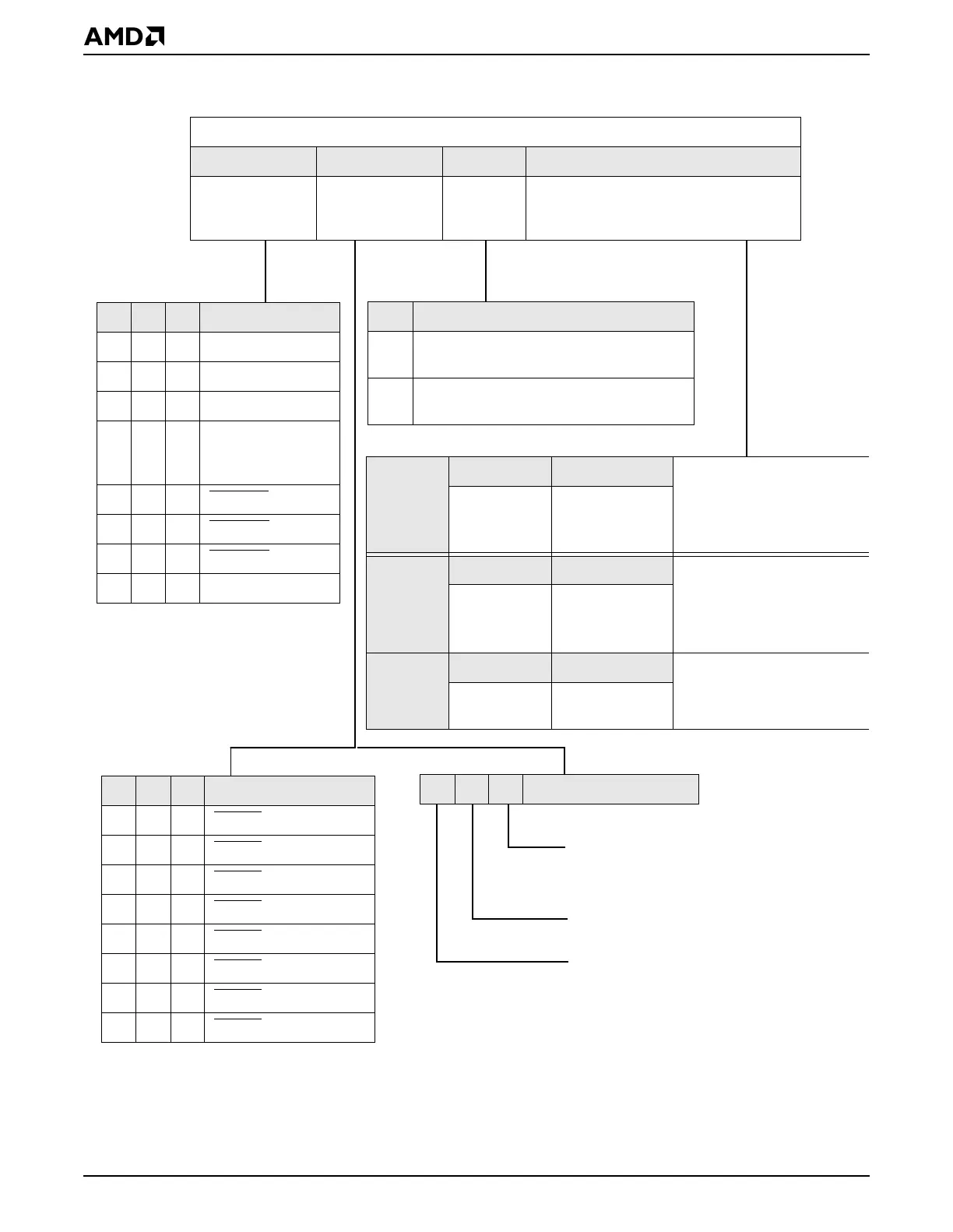
Figure 3-2 Programmable Address Region (PAR) Register Format
31 30 29 Target Device
0 0 0 Window disabled
0 0 1 GP bus I/O
0 1 0 GP bus memory
0 1 1 PCI bus (applies to
memory cycles to
PAR 0–PAR 1 only)
100BOOTCS
(ROM)
101ROMCS1
110ROMCS2
1 1 1 SDRAM
Programmable Address Region Register
31–29 28–26 25 24–0
Target of the
PAR Window
(TARGET)
Attribute
(ATTR)
Page Size
(PG_SZ)
Region Size/Start Address
(SZ_ST_ADR)
28 27 26 GP Bus Chip Select
0 0 0 GPCS0
0 0 1 GPCS1
0 1 0 GPCS2
0 1 1 GPCS3
1 0 0 GPCS4
1 0 1 GPCS5
1 1 0 GPCS6
1 1 1 GPCS7
28 27 26 ROM/SDRAM Attribute
0 = Write-enabled region
1 = Write-protected region
0 = Cacheable region
1 = Noncacheable region
0 = Code execution permitted
1 = Code execution denied
25 Memory Page Size
0 4-Kbyte memory page size on 4-Kbyte
boundary, ignored for I/O cycles.
1 64-Kbyte memory page size on 64-Kbyte
boundary, ignored for I/O cycles.
Memory
Cycle
When
[25]=0
24–18 17–0 Size defines up to 128
pages of 4-Kbyte size each,
on 4-Kbyte boundary, for a
512-Kbyte maximum win-
dow size.
Region Size
[6–0]
Start Address
A[29–12]
Memory
Cycle
When
[25]=1
24–14 13–0 Size defines up to 2K pages
of 64-Kbyte size each on 64-
Kbyte boundary, for a 128-
Mbyte maximum window
size.
Region Size
[10–0]
Start Address
A[29–16]
I/O
Cycles
Only
24–16 15–0 Size defines up to 512 bytes
with byte resolution in 64-
Kbyte I/O space.
Region Size
[8–0]
Start Address
A[15–0]
If Target is GP bus
If Target is ROM or SDRAM