Clock Generation and Control
Élan™SC520 Microcontroller User’s Manual 5-3
5.3 SYSTEM DESIGN
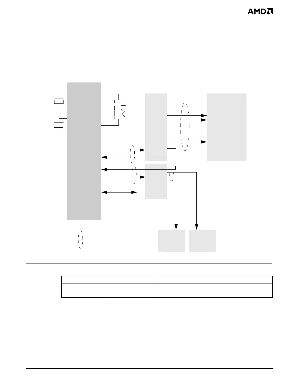
Figure 5-2 shows a system block diagram of the ÉlanSC520 microcontroller’s external
clocks. As shown in Figure 5-2, external clock drivers may be necessary when the system
presents a large capacitive load.
Table 5-2 lists the shared clock signals of the ÉlanSC520 microcontroller.
Figure 5-2 System Clock Distribution Block Diagram
Table 5-2 Clock Signals Shared with Other Interfaces
Default Function Alternate Function Control
CLKTIMER CLKTEST CLK_PIN_DIR bit in Clock Select (CLKSEL) register
(MMCR offset C26h)
SDRAM
66 MHz
PCI
Device
PCI
Device
33 MHz
32KXTAL2
33MXTAL1
33MXTAL2
32KXTAL1
32.768-kHz
33-MHz
Crystal
Crystal
[CLKTEST]
CLKPCIOUT
33 MHz
CLKMEMOUT
66 MHz
CLKMEMIN
CLKPCIIN
.
.
.
Programmable
Optional
VCC_ANLG
LF_PLL1
R1
C1C2
Élan™SC520
Microcontroller
CLKTIMER/
Note: Dotted line ovals, , signify frequency groups.
Driver
Optional
Clock
Driver
Clock