Write Buffer and Read Buffer
Élan™SC520 Microcontroller User’s Manual 11-3
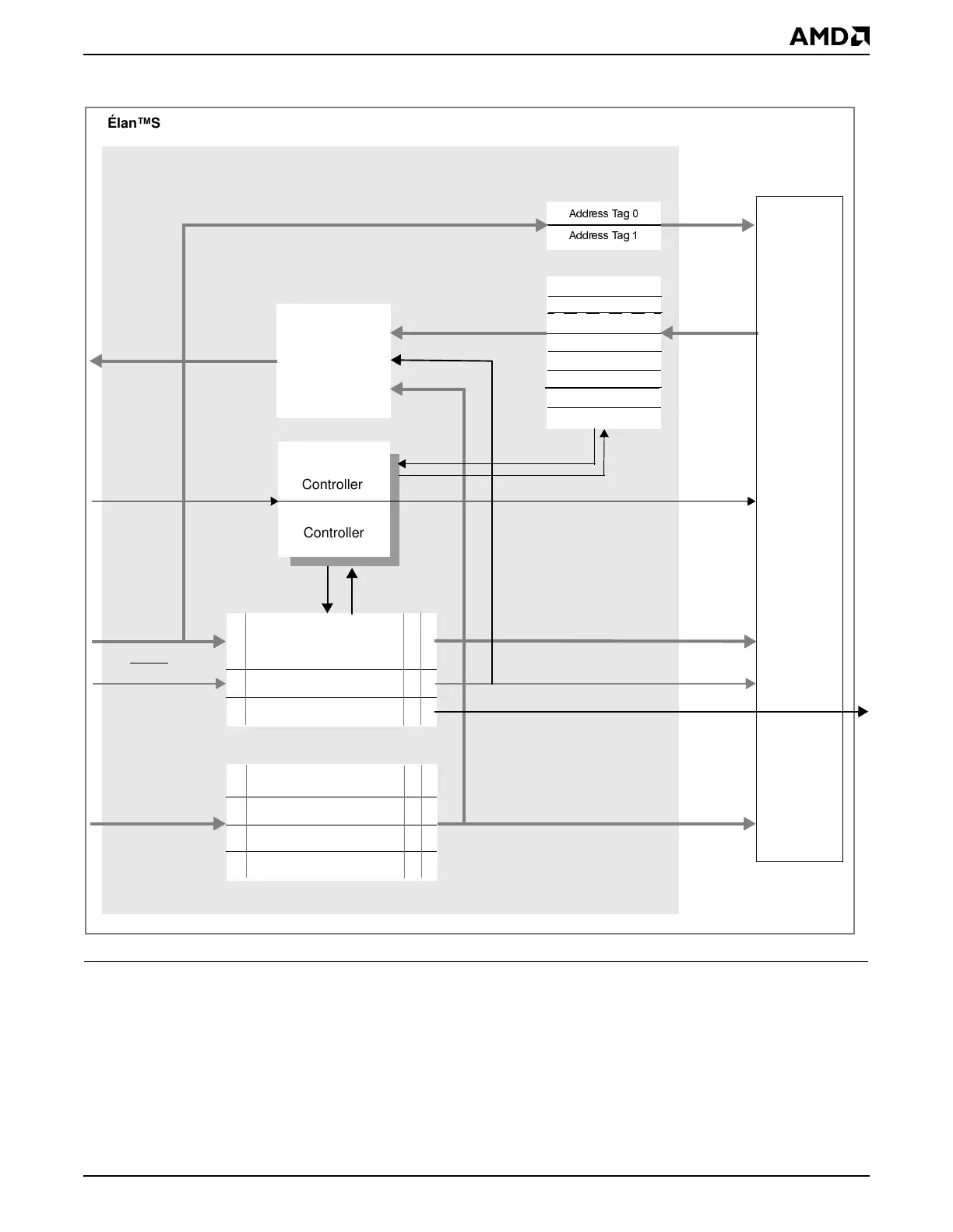
Figure 11-2 Write Buffer and Read Buffer Block Diagram
11.3 SYSTEM DESIGN
Table 11-1 shows the multiplexing of signals that are used for SDRAM trace support and
test. See Chapter 24, “System Test and Debugging”, for more information on the uses of
these pins.
The CFG2–CFG0 pinstrap functions associated with these three pins are sampled only as
a result of PWRGOOD assertion and do not affect the other functions of these pins, so they
Read-Merge
x5_wr_data[31–0]
Write Buffer
Address/Debug Tag Storage (32 ranks)
wb_data[31–0]
Address Tag
Byte Valid Bits
Master Trace Bits
wb_ad[27–2]
Byte 2
Byte 1
Data Store (32 ranks)
dram_control
x5_control
Byte 3
Byte 0
wb_be_l[3–0]
x5_be[3–0]
dram_
doubleword 6
doubleword 5
doubleword 7
doubleword 4
Address Latch
x5_rd_
rd_ad
x5_ad[27–2]
WBMSTR2–WBMSTR0
rab_data[31–0]
Read Buffer
31 01
doubleword 2
doubleword 1
doubleword 3
doubleword 0
$GGUHVV7DJ
$GGUHVV7DJ
Controller
Controller
Élan™SC520 Microcontroller
data[31–0]
data[31–0]
[27–2]
SDRAM
Controller
Write Buffer/Read Buffer
Read Buffer
Read Buffer Data Latch