System Address Mapping
4-4 Élan™SC520 Microcontroller User’s Manual
– GP bus I/O space (accessible only by the CPU)
– PCI bus I/O space (accessible by the CPU and PCI masters)
– PCI bus configuration space (accessible only by the CPU)
Table 4-4 summarizes the organization of memory and I/O address regions in the
ÉlanSC520 microcontroller.
4.3.1 Programming External Memory, Buses, and Chip Selects
Programming the external memory, buses, and chip selects on the ÉlanSC520
microcontroller is accomplished in three steps:
1. Configure the address space and any required attributes for the specified region.
2. Configure the timing, when applicable, and any required attributes of the interface.
3. For chip selects, enable the function on the desired pin by programming the pin
multiplexing in the PIO registers.
This chapter describes how to complete step 1. Programming the required timing and
attributes of the external interface (i.e., SDRAM, ROM, GP bus, or PCI bus) is accomplished
by writing to registers that control these interfaces. Finally, for chip selects, see Chapter 23,
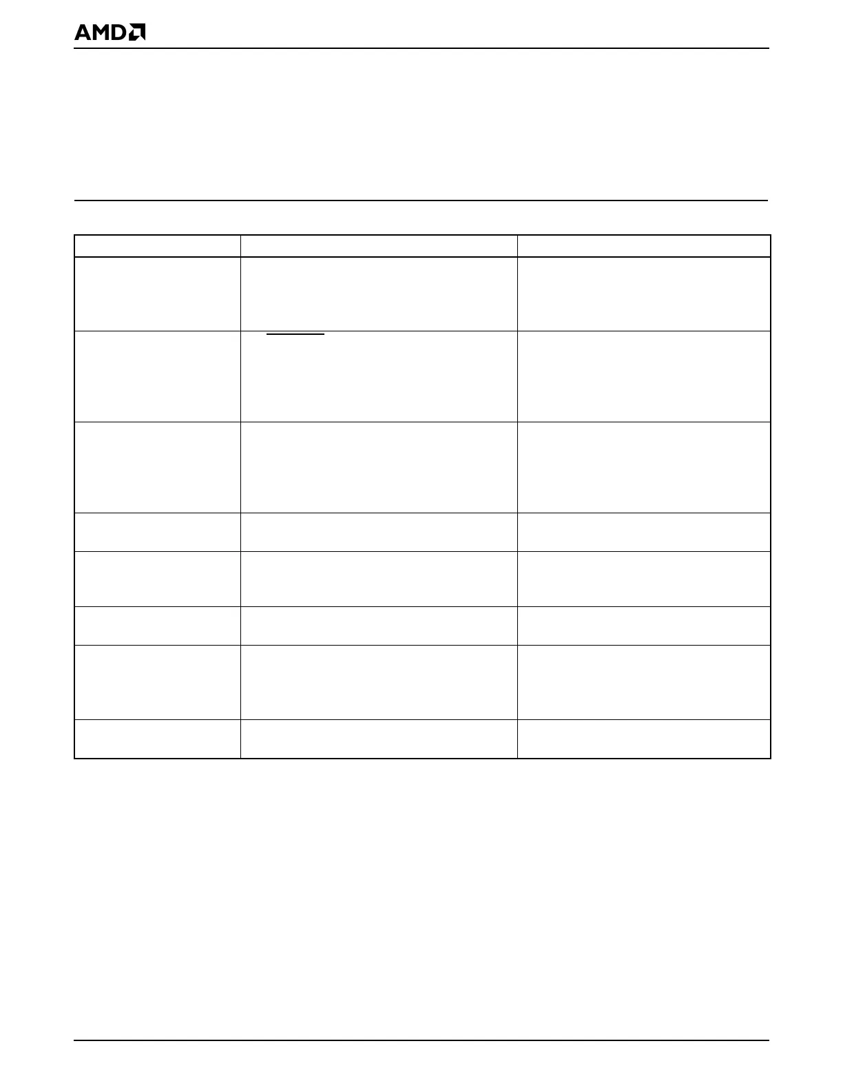
Table 4-4 Memory and I/O Space Summary
Device Memory Space I/O Space
SDRAM • Linear space starting at 00000000h to top
of SDRAM (maximum 256 Mbytes)
• PAR registers define noncacheable,
write-protected, nonexecutable regions
N/A
ROM/Flash • BOOTCS
mapped to CPU boot space
from FFFF0000–FFFFFFFFh
(64 Kbytes)
• PAR registers define noncacheable,
write-protected, nonexecutable regions
N/A
PCI Bus Normal Space • Default above SDRAM to top of memory
address space (4 Gbytes), minus boot
space (64 Kbytes) and MMCR (4 Kbytes)
• Two PAR registers can define any region
that overlays SDRAM space
Any space not claimed by CBAR, PC/AT
peripherals, GP bus (via PAR registers),
or PCI configuration registers (0CF8–
0CFFh)
PCI Bus Configuration
Space
N/A 0CF8–0CFFh
GP Bus Defined via PAR registers in lower 1 Gbyte Defined via PAR registers in lower 64
Kbytes, except for integrated
peripherals’ I/O space
Integrated PC/AT
Peripherals
N/A 0000h-03FFh
MMCR Registers • Defaults to 4-Kbyte region starting at
FFFEF000h
• CBAR can alias this to any 4-Kbyte
boundary in lower 1 Gbyte
N/A
Configuration Base
Address (CBAR) Register
N/A FFFC–FFFFh