Architectural Overview
Élan™SC520 Microcontroller User’s Manual 1-3
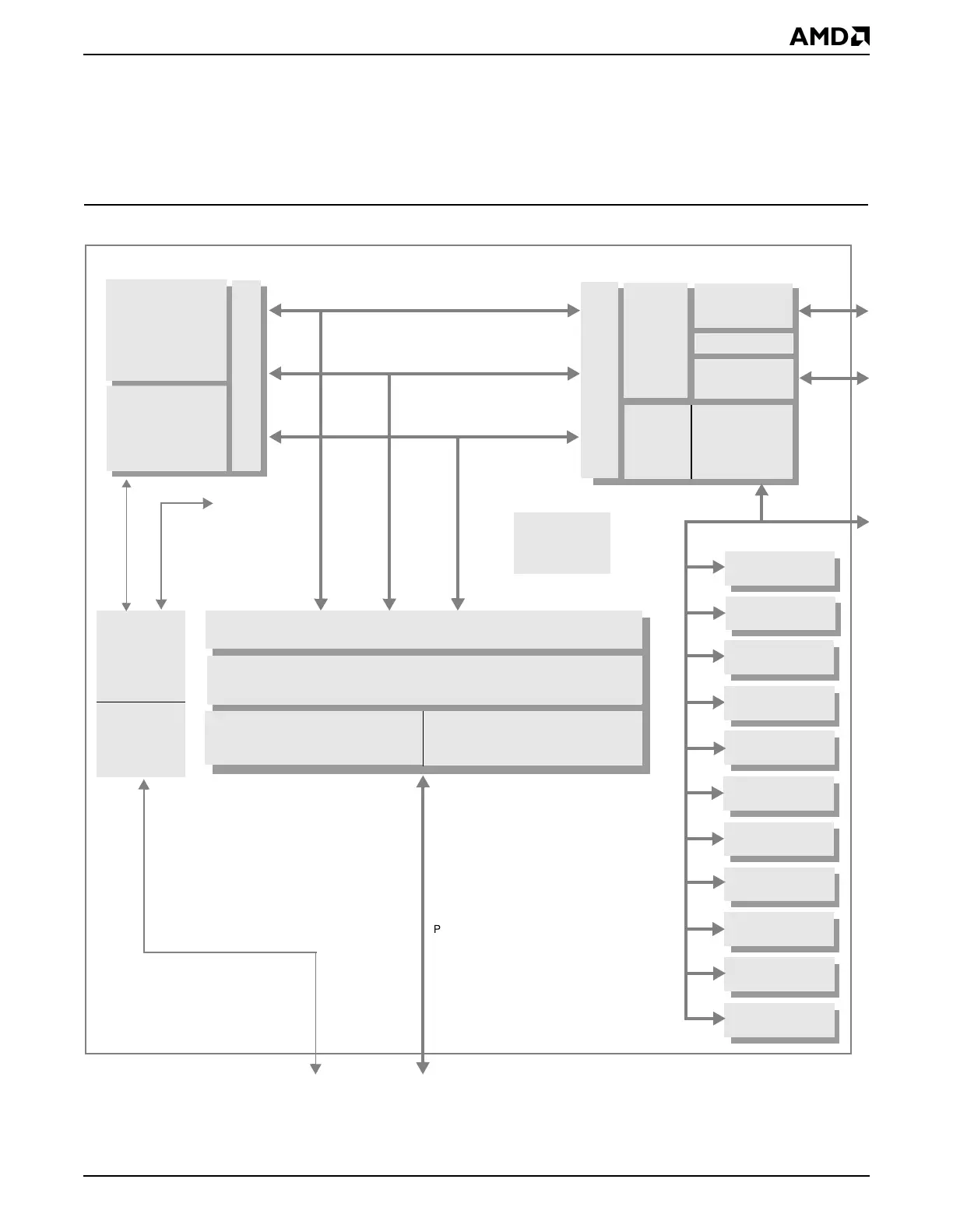
In addition to these three primary interfaces, the ÉlanSC520 microcontroller also contains
internal oscillator circuitry and phase locked loop (PLL) circuitry, requiring only two simple
crystals for virtually all system clock generation.
Diagrams showing how the ÉlanSC520 microcontroller can be used in various system
designs are included in “Applications” on page 1-8.
Figure 1-1 Élan™SC520 Microcontroller Block Diagram
Read/Write Buffers
Address
CPU Bus Interface
Am5
x
86
CPU
Bus Interface Unit
CPU Bus Interface
PCI
Target
PCI
Master
PCI Bus
Arbiter
CPU Bus
Arbiter
Clock
Generation
FIFOs and FIFO
Control
GP-DMA
Address
Data
Control/Status
CPU Data Bus
CPU Address Bus
CPU Control/Status Bus
GP Bus
AMDebug™
Technology and
JTAG
Request and
Grant
PCI Bus
PCI Requests and Grants
GP Bus
Controller
ROM/Flash
Controller
SDRAM
Controller
CPU
Request
External GP Bus
GP-DMA
Controller
Élan™SC520 Microcontroller
Programmable
Interrupt Controller
Programmable
Interval Timer
Watchdog Timer
Real-Time Clock
CMOS RAM
General-Purpose
Timers
Software
Timer
16550 UART
16550 UART
Synchronous Serial
Interface
Programmable I/O
Controls
PC/AT Compatibility
Logic
Decode
Unit