SDRAM Controller
Élan™SC520 Microcontroller User’s Manual 10-5
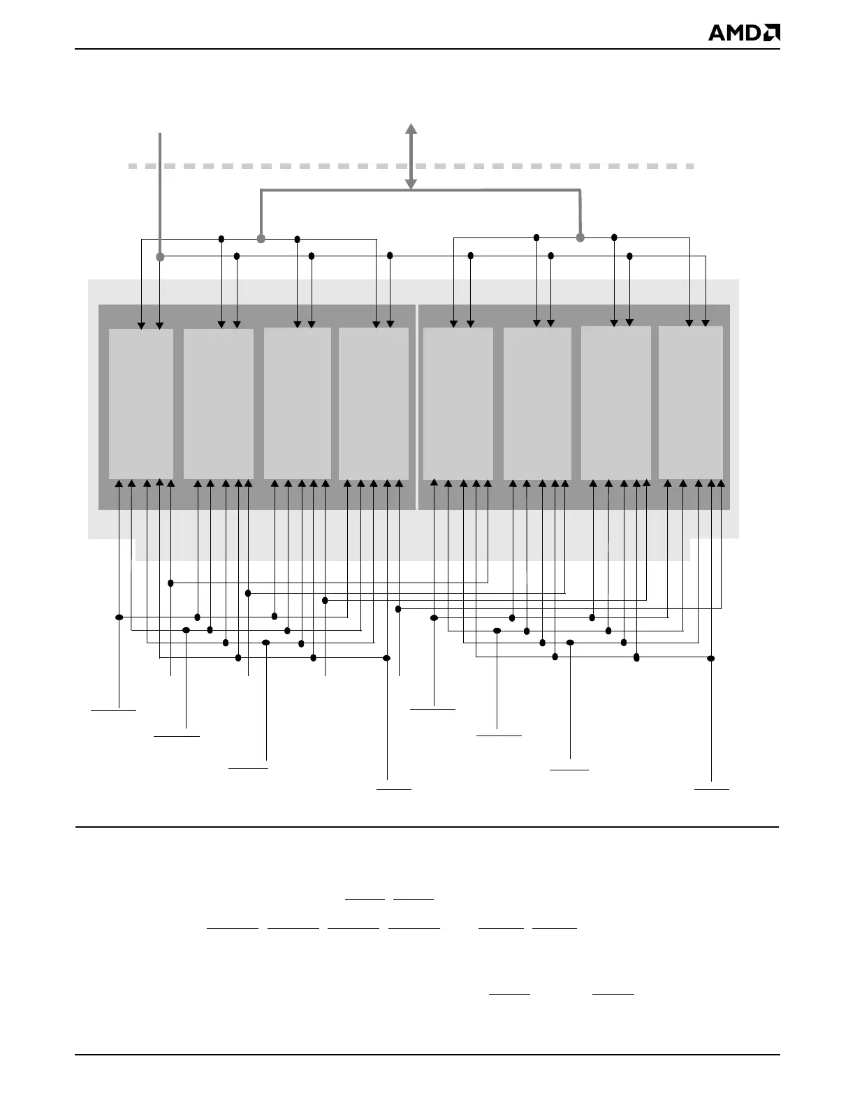
Figure 10-4 Example Configuration of a 168-Pin SDRAM DIMM
10.3.1 SDRAM Pins
The SDRAM interface pins are dedicated to supporting SDRAM devices only.
Four chip select signals, SCS3
–SCS0, are provided for independent bank selection.
The SRASA
–SRASB, SCASA–SCASB, and SWEA–SWEB signals are device command
signals that are encoded by the SDRAM controller to send a command to the SDRAM
devices. Each device in the array must sample these signals.
■ Since this may result in heavy loading, two SRAS and two SCAS signals are provided
to allow splitting load capacitance on these pins among the banks.
X8 X8
X8
X8 X8
X8
X8
X8
DQ63
–
DQ32 DQ31
–
DQ0
SCASB
SCASA
SRASB
SWEB
SCS1
SRASA
SWEA
SCS0
MD31
–
MD0
Bank 0
Bank 1
SDQM3
SDQM2 SDQM1
SDQM0
BA1
–
BA0
MA12
–
MA0,



 To Next Page