Programmable Interval Timer
16-2 Élan™SC520 Microcontroller User’s Manual
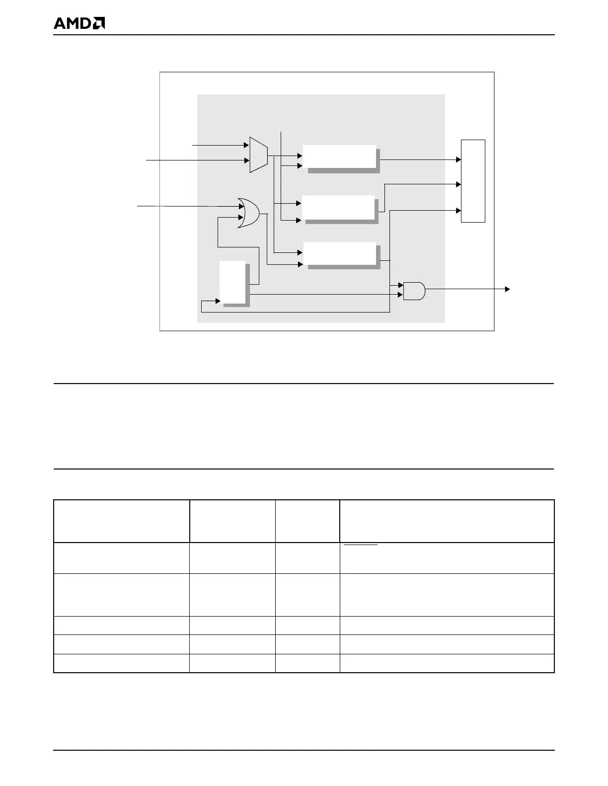
Figure 16-1 Programmable Interval Timer Block Diagram
16.4 REGISTERS
The programmable interval timer (PIT) is configured using the registers listed in Table 16-2
and Table 16-3. The direct-mapped System Control Port B register is used to provide PC/
AT-compatible PIT functionality.
Table 16-2 Programmable Interval Timer Configuration Registers—Memory-Mapped
Register Mnemonic
MMCR
Offset
Address Function
\\Chip Select Pin Function
Select
CSPFS C24h GPCS3
or PITGATE2 function select
\\Clock Select CLKSEL C26h CLKTIMER[CLKTEST] pin enable, clock output
select options (PIT), CLKTIMER select (input
clock for PIT)
\\PIT 0 Interrupt Mapping PIT0MAP D20h PIT 0 interrupt mapping
\\PIT 1 Interrupt Mapping PIT1MAP D21h PIT 1 interrupt mapping
\\PIT 2 Interrupt Mapping PIT2MAP D22h PIT 2 interrupt mapping
Channel 0
Channel 1
Channel 2
CLKTIMER
Programmable Interval Timer
gate 2
0061h[0]
0061h[5]
PITOUT2
0061h[1]
1.1882
Always Enabled
PITGATE2
pit_tmr1_irq
pit_tmr2_irq
gate 1
PIC
Port
pit_tmr0_irq
gate 0
B
MHz
Élan™SC520 Microcontroller
Notes:
Port B is addressed at 0061h in I/O space.