PCI Bus Host Bridge
Élan™SC520 Microcontroller User’s Manual 9-5
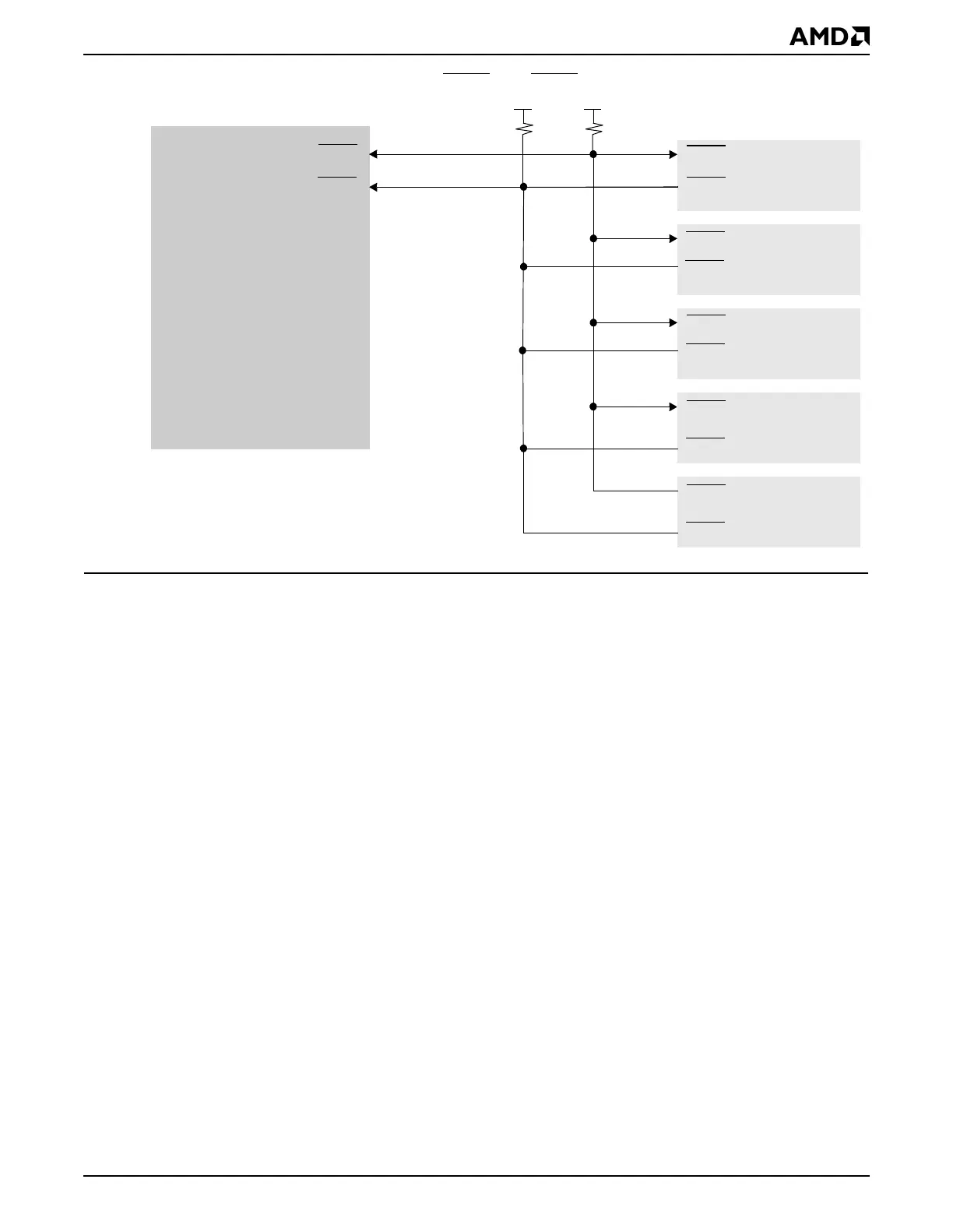
Figure 9-4 Élan™SC520 Microcontroller SERR and PERR Connection
9.3.1 PCI Clocking
The system PCI bus clock (CLK) is sourced from the ÉlanSC520 microcontroller. There
are two PCI bus clock pins on the ÉlanSC520 microcontroller: CLKPCIIN and CLKPCIOUT.
The CLKPCIOUT output pin drives a 33-MHz clock that is used as the system PCI bus
clock. However, the PCI host bridge logic is clocked from the CLKPCIIN input pin. The two
pins are provided for the PCI bus clock to minimize clock skew between the PCI host bridge
and external PCI bus devices.
The CLKPCIIN input pin guarantees that the PCI host bridge is driven with the same clock
as the external PCI bus devices. Otherwise, external buffering and loading of the
CLKPCIOUT pin could delay the clock, so that the skew between the PCI host bridge and
external PCI bus devices would not meet the PCI bus specification.
External buffering of CLKPCIOUT may or may not be required, depending on the system
loading (see Figure 9-5 and Figure 9-6). The ÉlanSC520 microcontroller does not
dynamically slow down or stop the output CLKPCIOUT clock; therefore the PCI bus
CLKRUN pin is not supported.
The CLKPCIIN pin is specifically intended for addressing the clock skew problem. It is
not
intended to enable running the PCI host bridge with a clock that is asynchronous to the
CLKPCIOUT pin. Driving the CLKPCIIN pin from an external source that is of a different
frequency is also not supported.
PERR
SERR
PERR
SERR
PERR
SERR
PERR
SERR
PERR
SERR
PCI Device 0
PCI Device 1
PCI Device 2
PCI Device 3
PERR
SERR
PCI Device 4
eODQ6&0LFURFRQWUROOHU