Boundary Scan Test Interface
Élan™SC520 Microcontroller User’s Manual 25-13
Notes:
The control cell for the BA1–BA0 and MA12–MA0 pins is closest to the JTAG_TDI pin (beginning
of the boundary scan chain), and TMROUT0 is closest to the JTAG_TDO pin (end of the boundary
scan chain).
Each of the shaded control cells shown in Table 25-3 contains the output enable control for the pads
listed below the control cell and before the next control cell. For bidirectional pads, the output is
listed first (closest to JTAG_TDI).
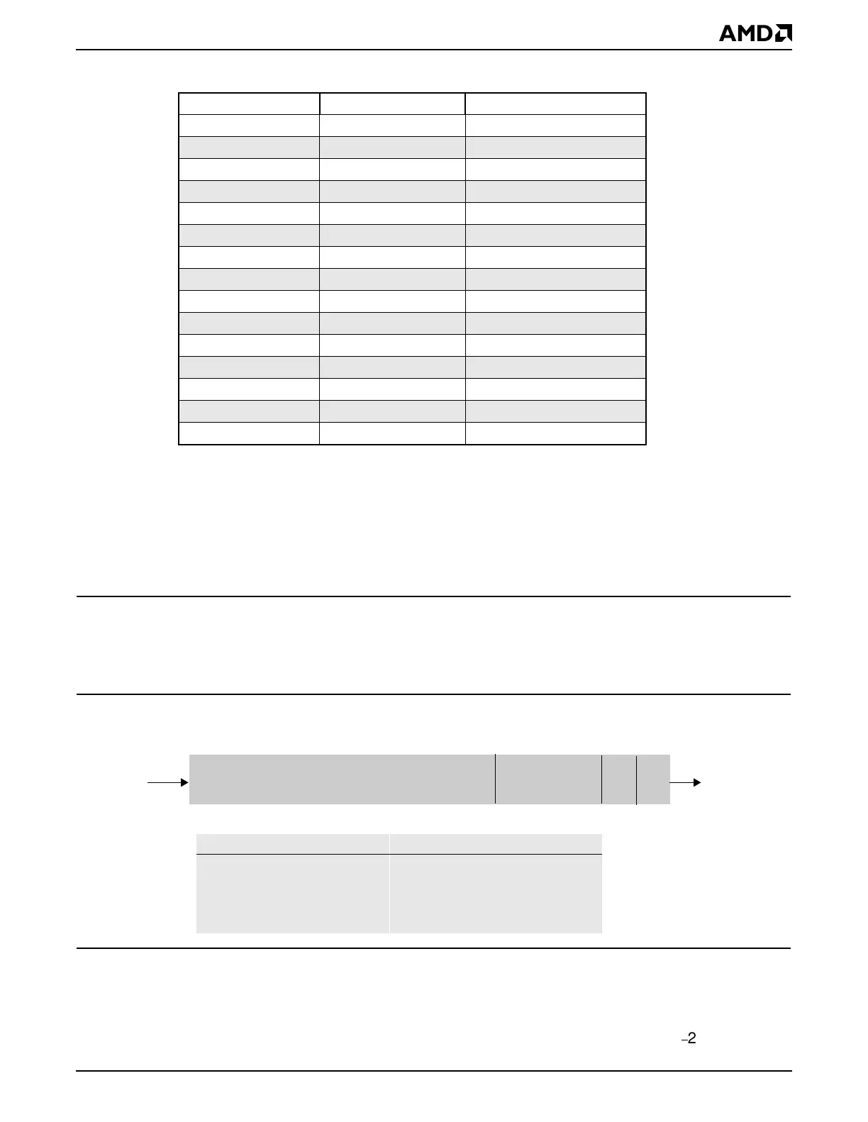
25.4.2.4 Serial Debug Port Data Register
Figure 25-2 shows the format of the Serial Debug Port Data register. The 38-bit Serial
Debug Port Data register serves as a command/status/data interface with the Am5
x
86 CPU.
Figure 25-2 Serial Debug Port Data Register Format
25.4.2.5 Device Identification Register
Figure 25-3 shows the format of the Device Identification register. For the ÉlanSC520
microcontroller, the least significant 28-bits of the Device Identification register are hard-
coded to a value of 0EFF003h. The VERSION field, represented by bits 31
±
28, reflects the
DATASTRB Bidirectional 467, 468
Control 469
CPUACT Bidirectional 470, 471
Control 472
PITOUT2 Bidirectional 473, 474
Control 475
PITGATE2 Bidirectional 476, 477
Control 478
TMRIN1 Bidirectional 479, 480
Control 481
TMRIN0 Bidirectional 482, 483
Control 484
TMROUT1 Output 485
Control 486
TMROUT0 Output 487
Table 25-3 Main Data Scan Path (Continued)
Pad Name Scan Type Boundary Scan Order
Debug Data
Command
PF
JTAG_TDO
JTAG_TDI
37
56
20
1
Bit Name Function
37–6 DEBUG_DATA[31–0] Debug Data
5–2 COMMAND[3–0] Command
1 P Command pending flag status
0 F Command finished flag status