ROM/Flash Controller
12-2 Élan™SC520 Microcontroller User’s Manual
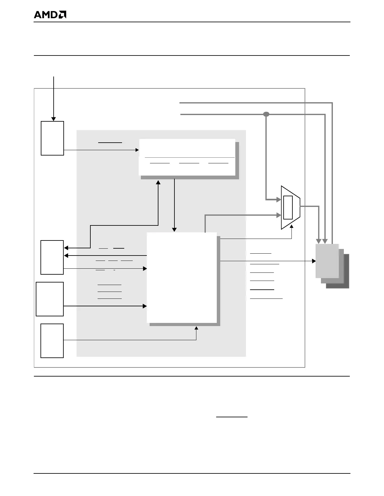
12.2 BLOCK DIAGRAM
Figure 12-1 shows a block diagram of the ROM controller.
Figure 12-1 ROM Controller Block Diagram
12.3 SYSTEM DESIGN
See the
Élan™SC520 Microcontroller Data Sheet
, order #22003, for timing tables and
additional timing diagrams.
Configuration information for the boot device (BOOTCS)
, specifically the width of the ROM
and the location of the ROM, is provided by external pinstrapping. The CFG2 pinstrapping
defines the bus, either SDRAM or GP bus data bus, on which the ROM is located. The
CFG1–CFG0 pins define the data width of the ROM devices. CFG2–CFG0 are latched
when PWRGOOD is asserted. See “Initialization” on page 12-14 for more information.
BOOTCS ROMCS1 ROMCS2
Configuration Registers
Configuration data
be3
–be0, blast,
rdy,
ROMRD
FLASHWR
BOOTCS
PAR
CPU
ROM Controller
ROMCS1
*
ROMCS2
*
BOOTCS
ROMCS1
ROMCS2
ROMBUFOE
Clock
cpu_clk (33 MHz)
Configuration data
wr_protect
ken
Reset
Pinstrap data
for BOOTCS
CFG2–CFG0
M
u
x
rom_cycle
GPA25–GPA0
address[3–0]
GPA3–GPA0
GPA25–GPA4
Data Bus (GPD15–GPD0 or MD31–MD0)
brdy
ads, w/r, x5_ad[3–2]
Élan™SC520 Microcontroller
Registers
ROM
Programmable
Timing Control
*May be multiplexed
with other pin
functions.