AMDebug™ Technology
Élan™SC520 Microcontroller User’s Manual 26-3
There are two AMDebug connector formats specified: a 12-pin connector (Figure 26-2) and
a 20-pin connector (Figure 26-3). They differ in maximum operating frequency and number
of connector pins. They both have the same number of active signals, but the 20-pin version
has a ground wire placed between each signal wire.
.
Software development systems based on the integrated debug technology should consider:
■ Providing for at least a 12-pin connector on each board design
■ Assigning the necessary tracking from the processor’s pins supporting the AMDebug
port to the standard 12-pin connector
■ Including the small connector on production systems to enable in-field debugging
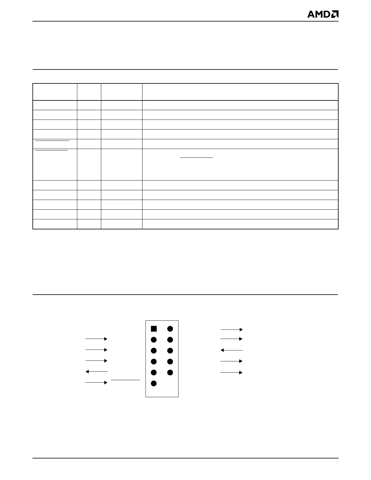
Figure 26-2 12-Pin Connector Format
Table 26-1 AMDebug™ Technology Connector Pins
Name I/O
External
Resistor Description
JTAG_TCK Input PU Clock for the TAP controller and the debug serial/parallel interface
JTAG_TDI Input PU Input test data and instructions
JTAG_TDO Output PU Output data; three-stated when data is not driven
JTAG_TMS Input PU Test functions and sequence of test changes
JTAG_TRST
Input PU Reset the JTAG controller
SYSRESET
Input PU Reset all system logic. This pin should be held Low for at least four TCK
clock cycles. SYSRESET
can be ANDed directly with the PWRGOOD
signal. This enables the AMDebug control unit to drive the ÉlanSC520
microcontroller’s reset.
BR/TC Input PD Request entry to AMDebug mode/Turn instruction trace capture on-off
CMDACK Output — Acknowledge command
STOP/TX Output — Asserted High on entry to AMDebug mode; during normal mode set High
TRIG/TRACE Output — Trigger event to logic analyzer (optional, from Am486 debug registers)
PWRGOOD Output — Sample power level used by the JTAG controller driving hardware
Ground
Test Clock
Test Mode Select
Test Data In
Test Data Out
Reserved for
System Reset
Sample Power Source
Command Acknowledge
Trigger Event
V
GND
JTAG_TCK
JTAG_TMS
JTAG_TDI
JTAG_TDO
SYSRESET
PWRGOOD
CMDACK
BR/TC
STOP/TX
TRIG/TRACE
Keyed
12
12
In AMDebug Mode, Receive Data
Enter AMDebug Mode, Trace Control