GP Bus DMA Controller
Élan™SC520 Microcontroller User’s Manual 14-3
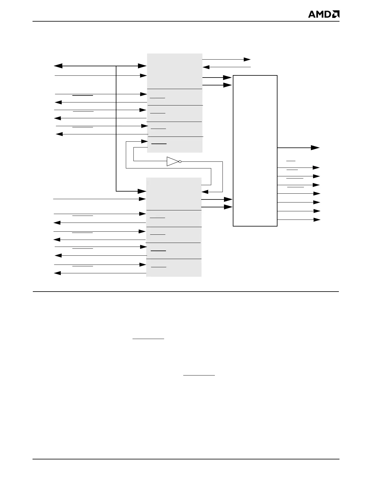
Figure 14-2 Master and Slave Core Cascading Diagram
14.3 SYSTEM DESIGN
Table 14-1 shows GP-DMA signals shared with other interfaces. When enabled, the
multiplexed signals shown in Table 14-1 either disable or alter any other function that uses
the same pin.
The GPDRQx and GPDACKx
signals have programmable polarities. The default polarity
is compatible to the ISA convention.
Since the GP-DMA controller does not generate an interrupt at the end of the transfer,
system designers can externally connect GPTC to any GPIRQx to trigger an interrupt. Note
that qualifying GPTC with a specific GPDACKx
signal provides a more specific interrupt.
For an application that requires a DMA transfer every fixed interval of time, a timer output
(TMROUT1 or TMROUT0) can be connected to the GPDRQx pin.
See the
Élan™SC520 Microcontroller Data Sheet
, order #22003, for timing tables and
additional timing diagrams.
Master Core
HLDA
HRQ
bgnt
breq
DATA[7–0]
ADDR[15–0]
CS
HLDA
HRQ
DATA[7–0]
CS
dma1_cs
dma0_cs
Slave Core
gpdrq7
gpdack7
GP data
Interconnect
Logic
dior
diow
dmemr
dmemr
GPTC
GPAEN
Channel 7
DRQ
DACK
Channel 6
DRQ
DACK
Channel 5
DRQ
DACK
Channel 4
DRQ
DACK
Channel 3
DRQ
DACK
Channel 2
DRQ
DACK
Channel 1
DRQ
DACK
Channel 0
DRQ
DACK
gpdrq6
gpdack6
gpdrq5
gpdack5
gpdrq3
gpdack3
gpdrq2
gpdack2
gpdrq1
gpdack1
gpdrq0
gpdack0
ADDR[15:0]
daddr[27–0]
dma_is_16
ADDR[15–0]