General-Purpose Bus Controller
Élan™SC520 Microcontroller User’s Manual 13-13
13.5.8.2 Interfacing with a Super I/O Controller
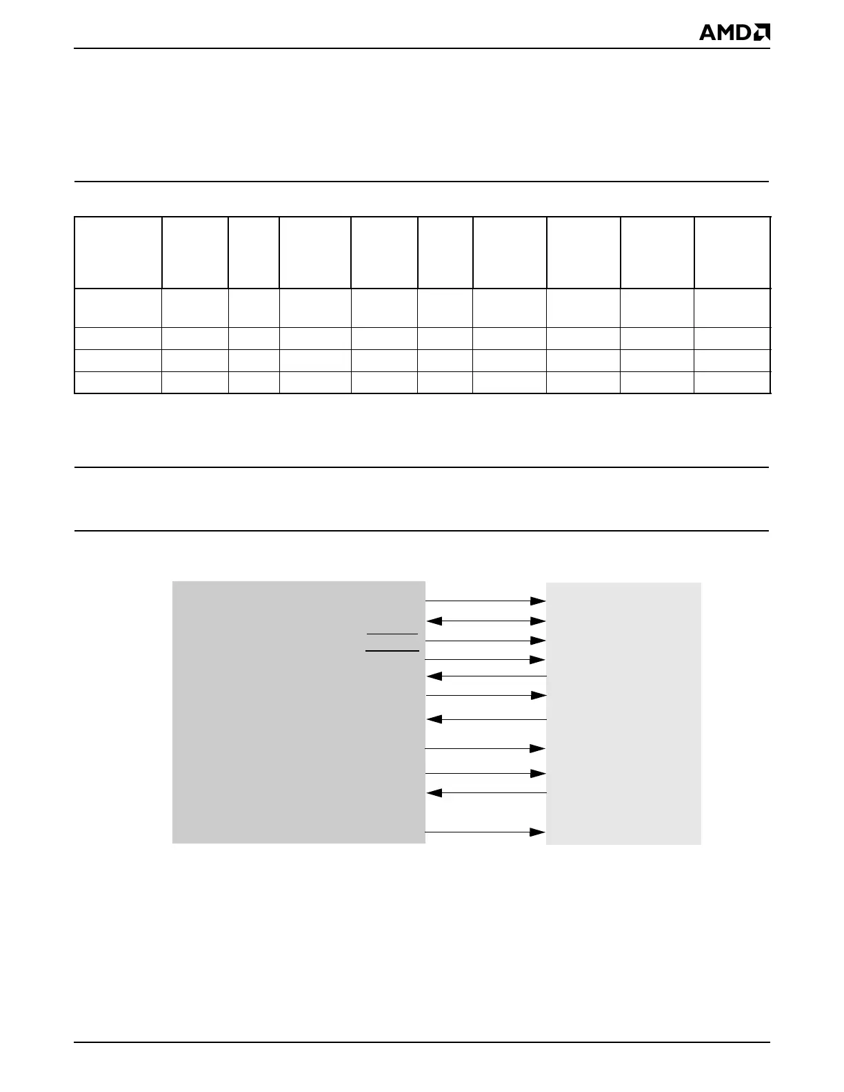
Figure 13-5 shows an example system diagram of the ÉlanSC520 microcontroller
interfacing with a Super I/O controller. Figure 13-6 shows the interfacing timing example.
In this example, the programmable interface timing registers can be programmed as shown
in Table 13-5, using the equation from “Programmable Bus Interface Timing” on page 13-7:
Note that the bus cycle can be stretched out by deasserting GPRDY; see “Wait States” on
page 13-20 for more information.
Figure 13-5 Élan™SC520 Microcontroller Interfacing with a Super I/O Controller
Table 13-5 Example Super I/O Controller Interface Timing
1
Notes
1. This example assumes that a 33.333-MHz crystal is being used in the system.
GP Bus
Signal Type
Offset
Register
Value
Offset
Time
(ns)
Chip
Require-
ment (ns)
Pulse
Width
Register
Value
Pulse
Width
(ns)
Chip
Require-
ment (ns)
Recovery
Time
Register
Value
Recovery
Timer
(ns)
Chip
Require-
ment (ns)
GP chip
selects
0 30 N/A 0 30 N/A 2 90 66
GP read 0 30 19 1 60 60 N/A N/A N/A
GP write 0 30 19 1 60 60 N/A N/A N/A
GPALE 0 30 N/A 0 30 N/A N/A N/A N/A
SD7–SD0
IORJ
IOWJ
SA10–SA0
MR
IOCHRDY
GPD7–GPD0
GPIORD
GPIOWR
GPA10–GPA0
GPRESET
GPRDY
DRQ3J–
GPDRQx
DACK3J–
TC
GPTC
IRQ7–3
GPIRQx
DRQ1J
DACK1J
GPDACKx
AEN
GPAEN
IRQ11–9
Élan™SC520 Microcontroller
Super I/O